Back-illuminated Si-PIN photoelectric detector taking black silicon material as photosensitive layer and manufacturing method thereof

A photodetector and photosensitive layer technology, applied in the field of photoelectric detection, can solve the problems of poor thermomechanical properties, poor crystal quality, and high price, and achieve the effects of low cost, high light absorption rate, and simple preparation process

Active Publication Date: 2011-09-07
UNIV OF ELECTRONICS SCI & TECH OF CHINA
View PDF1 Cites 25 Cited by
  • Summary
  • Abstract
  • Description
  • Claims
  • Application Information

AI Technical Summary

Problems solved by technology

However, InGaAs single crystal semiconductor materials have disadvantages such as high price, poor thermomechanical properties, poor crystal quality, and not easy to be compatible with existing silicon microelectronics processes.

Method used


Image

  • Back-illuminated Si-PIN photoelectric detector taking black silicon material as photosensitive layer and manufacturing method thereof
  • Back-illuminated Si-PIN photoelectric detector taking black silicon material as photosensitive layer and manufacturing method thereof
  • Back-illuminated Si-PIN photoelectric detector taking black silicon material as photosensitive layer and manufacturing method thereof

Examples


Embodiment Construction

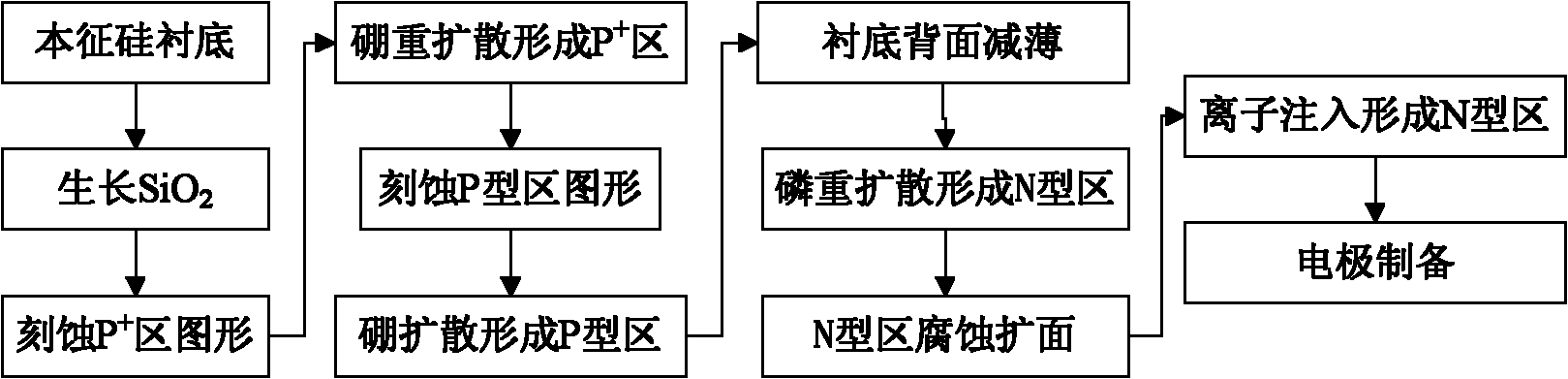
[0022] The specific implementation method of the present invention will be further described below in conjunction with the drawings and embodiments.

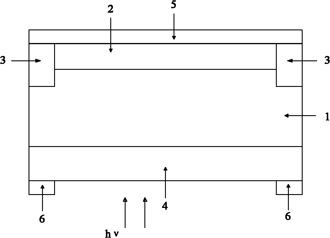
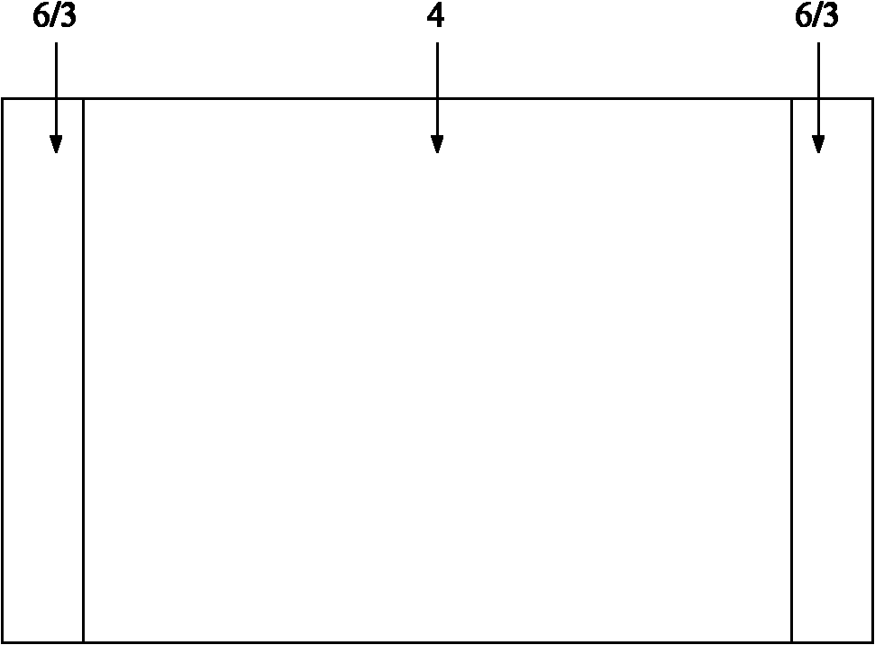
[0023] A back-illuminated Si-PIN photodetector with black silicon material as the photosensitive layer, such as figure 1 , 2 As shown, it includes a silicon intrinsic substrate 1, a P-type region 2 located in the center of the front surface of the silicon intrinsic substrate 1, and an annular P-type region located around the front surface of the silicon intrinsic substrate 1. + Region 3, N-type black silicon layer 4 located on the back side of silicon intrinsic substrate 1, located in P-type region 2 and P + The upper electrode 5 on the upper surface of the region 3, and the lower electrodes 6 located on both sides of the lower surface of the N-type black silicon layer 4; wherein P + The junction depth of region 3 is greater than the junction depth of P-type region 2 .

[0024] Among the above technical solutions:

[0025] T...


PUM


Abstract

The invention discloses a back-illuminated Si-PIN photoelectric detector taking a black silicon material as a photosensitive layer and a manufacturing method thereof, belonging to the technical field of photoelectric detection. The photoelectric detector comprises a silicon intrinsic substrate, a P-type area located in the centre of the front surface of the silicon intrinsic substrate, an annularP+ area located around the front surface of the silicon intrinsic substrate, an N-type black silicon layer located on the back surface of the silicon intrinsic substrate, upper electrodes located on the upper surface of the P-type area and the P+ area, and lower electrodes located on the two sides of the lower surface of the N-type black silicon layer. According to the invention, the black silicon material is used as the photosensitive layer, and an annular P+ area 3 is increased around the P-type area 2 so that the back-illuminated Si-PIN photoelectric detector disclosed by the invention canabsorb light waves of near-infrared band and has higher light absorptivity and wider response band than a traditional Si photoelectric detector; the manufacturing process is relatively simple and hasthe characteristics of low cost, fast response speed, high responsiveness and wide response band, is easy to realize integration, and has obvious advantages in large-scale marketization.

Description

technical field [0001] The invention belongs to the technical field of photoelectric detection, and relates to the structure of a photoelectric detection device, in particular to a back-illuminated Si-PIN photoelectric detector and a preparation method thereof. Background technique [0002] As an important part of optical fiber communication system, infrared imaging system, laser warning system and laser ranging system, photoelectric detectors have been widely used in civilian and military applications. Currently widely used photodetectors mainly include photodetectors for detecting wavelengths ranging from 400nm to 1100nm and InGaAs photodetectors for detecting wavelengths ≥ 1100nm. Among them, Si material is the most widely used material in the semiconductor industry due to its advantages such as easy purification, easy doping, abundant resources, low cost, easy large-scale integration, and mature related technologies. However, due to its large forbidden band width (1.12e...

Claims


Application Information

Patent Timeline
Patent Type & Authority Applications(China)
IPC IPC(8): H01L31/028H01L31/0352H01L31/075H01L31/18
CPCY02E10/50Y02E10/547Y02E10/548Y02P70/50
Inventor 李伟黄璐赵国栋吴志明蒋亚东
Owner UNIV OF ELECTRONICS SCI & TECH OF CHINA
Why Eureka
Try Eureka