Preparation method of nano-gap electrode in micro-nano electromechanical device

A technology of nano-gap electrodes and electrode materials, which is applied in the direction of microstructure technology, microstructure devices, and manufacturing microstructure devices, etc. It can solve the problems of high price, difficulty in large-scale manufacturing, and difficult control of the preparation process, and achieve high integration. , the effect of repeatable process

Inactive Publication Date: 2011-09-14
PEKING UNIV
View PDF7 Cites 14 Cited by
  • Summary
  • Abstract
  • Description
  • Claims
  • Application Information

AI Technical Summary

Problems solved by technology

Among them, (1) the electron beam has a shorter wavelength than ordinary light, and can obtain higher resolution due to the use of electric field to focus precisely, and can write directly under the control of the computer, but the efficiency is low and the price is expensive, and The proximity effect caused by the incident electron beam makes it difficult to apply on a large scale; (2) the advantage of the contact fracture method is that the method is simple, and electrodes with small gaps can be prepared, but it is not easy to mas

Method used


Image

  • Preparation method of nano-gap electrode in micro-nano electromechanical device
  • Preparation method of nano-gap electrode in micro-nano electromechanical device
  • Preparation method of nano-gap electrode in micro-nano electromechanical device

Examples


Embodiment Construction

[0018] The present invention will be further described below in conjunction with the examples, but the present invention is not limited to the following examples.

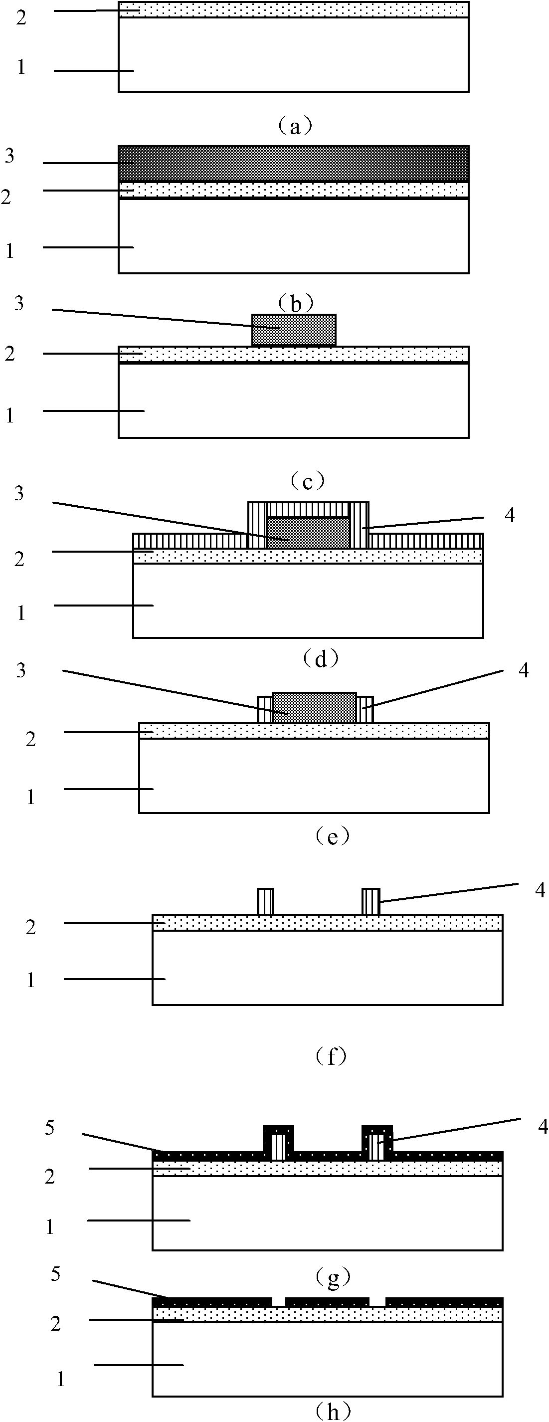
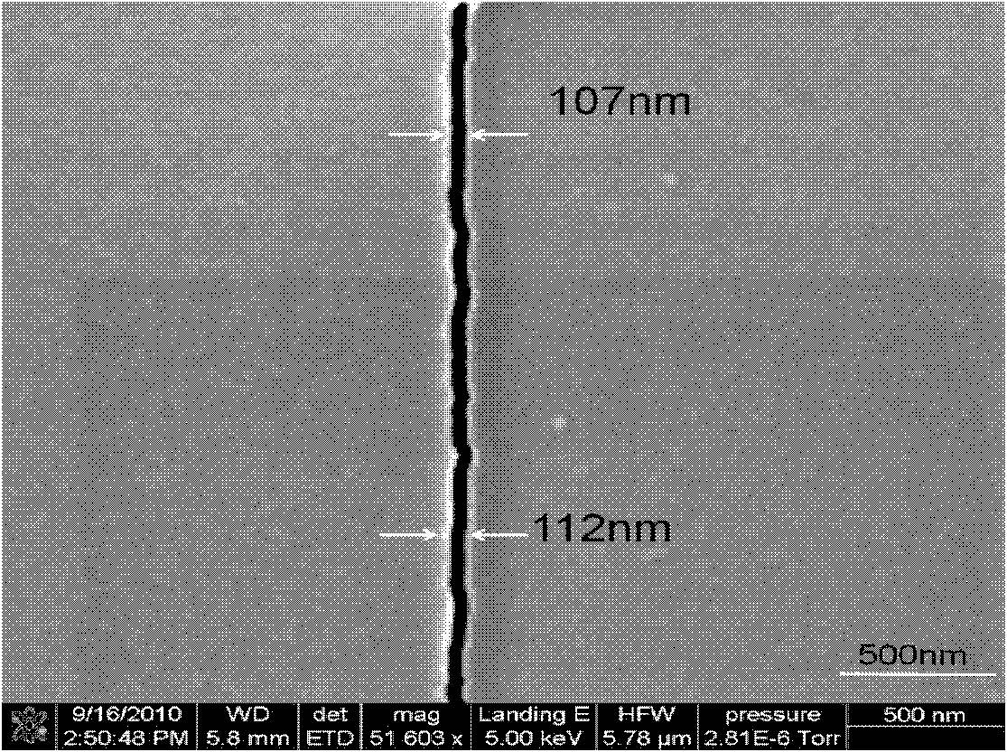
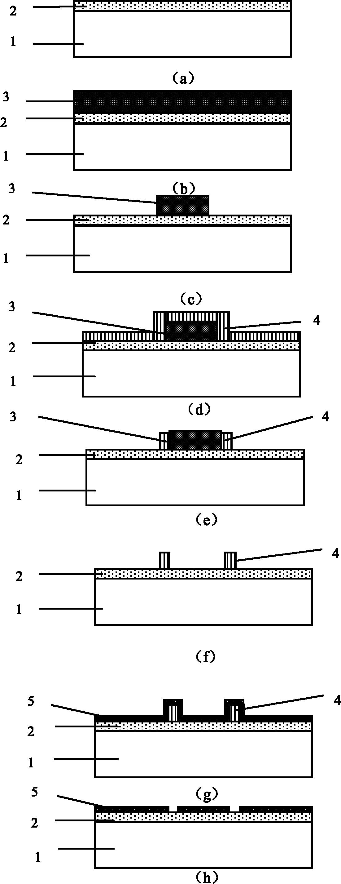
[0019] figure 1 The process flow chart for fabricating nano-metal gaps on silicon substrates is shown, and the specific steps are as follows:

[0020] 1) LPCVD thickness of 100nm to 120nm silicon nitride layer 2 on the silicon substrate 1, as the insulating layer of the metal electrode, see figure 1 (a);

[0021] 2) LPCVD deposits a polysilicon layer 3 with a thickness of 800nm, as an auxiliary structural layer 3 for subsequent oxide layer deposition, see figure 1 (b);

[0022] 3) After photolithography and development, use photoresist as a mask to dry-etch the polysilicon layer, and use ASE to form an auxiliary structural pattern with steep side walls, which is convenient for the subsequent deposition of the side wall sacrificial layer 4, such as figure 1 (c);

[0023] 4) LPCVD deposits a silicon oxide layer ...


PUM

PropertyMeasurementUnit
Thicknessaaaaaaaaaa
Thicknessaaaaaaaaaa

Abstract

The invention provides a preparation method of a nano-gap electrode in a micro-nano electromechanical device, which belongs to the field of micro-nano electromechanical systems. According to the preparation method, an appropriate material is selected to prepare a sacrificial layer, and the preparation method comprises the following steps of: firstly, preparing a nano-scale side wall structure of the sacrificial layer in a mode of back etching, wherein the side wall needs to have a certain height; secondly, depositing a layer of thin metal layer or other electrode materials; and thirdly, selectively corroding the side wall material of the sacrificial layer, wherein the metals or other electrode materials attached to the side wall are corroded together, and a gap is formed at the position of the side wall. The nano-gap electrode is prepared by keeping the thickness of the sacrificial layer side wall in a nano scale. The preparation method is compatible with the conventional semiconductor processing technique, is easy for large-scale production, and is low in cost.

Description

technical field [0001] The invention relates to a method for preparing a nano-gap electrode in a micro-nano electromechanical device, belonging to the field of micro-nano electromechanical systems. Background technique [0002] With the reduction of the feature size of silicon devices, the demand for the fabrication process of micro-nano structures is increasing. Nanogap electrodes are a fundamental part of MEMS devices. Nanogap electrodes have important applications in detecting the properties of nanoscale materials, as well as constructing quantum devices and biosensors. [0003] The process methods for manufacturing nano-gap electrodes include electron beam etching method, atomic force microscope nano-etching method, contact fracture method and electroplating method. Among them, (1) the electron beam has a shorter wavelength than ordinary light, and it can obtain higher resolution due to the use of electric field to focus precisely, and can write directly under the cont...

Claims


Application Information

Patent Timeline
IPC IPC(8): B81C1/00
Inventor 于晓梅于侃王晓菲
Owner PEKING UNIV
Why Eureka
Try Eureka