Equipment and method for preparing high-purity directionally crystallized polysilicon

A technology of directional crystallization and polysilicon, applied in polycrystalline material growth, chemical instruments and methods, crystal growth, etc., can solve problems such as crucible material pollution, achieve low cost, reduce production cost, and solve the difficult effect of waterway design

Active Publication Date: 2011-09-21
SHENZHEN SUMMIT LEVITATION METALLURGICAL SCI & TECHN
View PDF6 Cites 10 Cited by
  • Summary
  • Abstract
  • Description
  • Claims
  • Application Information

AI Technical Summary

Problems solved by technology

[0006] The technical problem to be solved by the present invention is: the crucible material will produce pollution when polysilicon is prepared by directional solidification casting technology. The present invention combines induction cold crucible technology with directional solidification casting technology to obtain cold crucible directional solidification technology. Contamination by crucible material

Method used


Image

  • Equipment and method for preparing high-purity directionally crystallized polysilicon
  • Equipment and method for preparing high-purity directionally crystallized polysilicon
  • Equipment and method for preparing high-purity directionally crystallized polysilicon

Examples


preparation example Construction

[0080] The present invention also proposes a preparation method for preparing high-purity directional crystal polysilicon with the above-mentioned equipment, which includes the following steps:

[0081] Step 1: Preparatory work: raise the crucible bottom 24 of the cold crucible 2 to the lower part of the cold crucible 2, seal the lower opening of the cold crucible 2, then add the metal silicon raw material to be purified into the cold crucible 2, to accommodate the cold crucible Vacuumize the vacuum chamber 1 of 2, and fill the vacuum chamber 1 with high-purity inert gas, such as high-purity argon with a purity of not less than 99.999%, after the vacuum degree reaches the requirement;

[0082] Step 2: Start the heating and melting process: In order to carry out the directional solidification process, the induction power supply must first be activated to deliver high-frequency current to the main inductor 3 surrounding the cold crucible 2 and generate an electromagnetic field in...

Embodiment 1

[0088] Embodiment 1 is an example of preparing polysilicon.

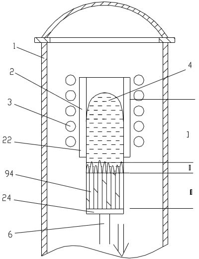
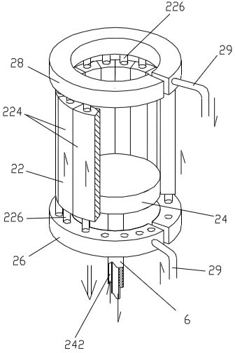
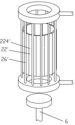
[0089] Vacuum chamber 1 is made of stainless steel ( figure 1 ), inner diameter 600mm, height 2.5m. The internal diameter of cold crucible 2 is 200mm, and height is 800mm ( image 3 ). The crucible wall is divided into 22 parts and 24 petals, and the outer surface is welded with copper tubes for water cooling. A movable crucible bottom 24 is mounted on the lower end of the crucible wall 22 . The power supply is 350kw and the frequency is 10kc. It is connected to the main inductor 3 surrounding the cold crucible 2 .

[0090] The crystallization zone is located in the section of the auxiliary inductor 46 at 20 mm below the lower end of the crucible wall 22 ( Figure 5 ). The auxiliary inductor 46 has an inner diameter of 210mm and a height of 100mm, which is connected with an auxiliary power supply with a power of 60kw and a frequency of 400kc. The high-frequency electromagnetic field in the crystallization zon...


PUM

PropertyMeasurementUnit
purityaaaaaaaaaa

Abstract

The invention relates to equipment for preparing high-purity directionally crystallized polysilicon. The equipment comprises a vacuum chamber, a cold crucible, a main inductor, a crystallizing device and a cooler, wherein the cold crucible is arranged in the vacuum chamber and made of red copper; the cold crucible comprises a cylindrical crucible wall and a crucible bottom separated from the crucible wall; the crucible wall is partitioned into a plurality of crucible blades; each crucible blade is provided with a cooling water path; a water inlet sleeve and a water returning sleeve are arranged on the lower surface and the upper surface of the cold crucible respectively; the crucible bottom can move below the crucible wall; the main inductor is encircled outside the cold crucible; the crystallizing device is an auxiliary inductor arranged below the main inductor or the crystallizing device comprises a ceramic tube and a temperature preservation layer; the ceramic tube is arranged at the lower end of the crucible wall of the cold crucible; the temperature preservation layer is wrapped or encircled on the ceramic tube; and the cooler is arranged below the crystallizing device. The equipment is free of pollution and high in production efficiency. The invention also provides a method for preparing the high-purity directionally crystallized polysilicon by using the equipment.

Description

technical field [0001] The invention relates to a device for preparing high-purity polysilicon and a preparation method thereof, in particular to a device for preparing high-purity directional crystal polysilicon by induction cold crucible technology and a preparation method thereof. Background technique [0002] Silicon is one of the most important building blocks of modern technology. The most important examples include: the chips of computer technology and communication technology are based on monocrystalline silicon wafers, and photovoltaic technology uses polycrystalline silicon wafers and silicon thin films as photoelectric conversion materials. [0003] Although silicon is the most abundant element on the earth, the silicon used in high-tech fields must reach a very high purity. Polysilicon for photovoltaic technology should reach a purity of 6N, while the purity of monocrystalline silicon for chips should be higher than 9N. To achieve such purity requires the use of...

Claims


Application Information

Patent Timeline
Patent Type & Authority Applications(China)
IPC IPC(8): C30B28/06C30B29/06C01B33/037
Inventor 李碚张森
Owner SHENZHEN SUMMIT LEVITATION METALLURGICAL SCI & TECHN
Why Eureka
Try Eureka