Silicon on insulator (SOI) pressure resistant structure with interface lateral variation doping

A voltage-resistant structure and variable doping technology, applied in semiconductor devices, electrical components, circuits, etc., can solve the problems of large leakage current and poor reproducibility of SIPOS process, and achieve the effect of improving vertical withstand voltage

Inactive Publication Date: 2011-09-21
CHONGQING UNIV
View PDF5 Cites 6 Cited by
  • Summary
  • Abstract
  • Description
  • Claims
  • Application Information

AI Technical Summary

Problems solved by technology

The existing problems are the poor reproducibility of the SIPOS process and large leakage current; Literature: Guo Yufeng, Li Zhaoji, Zhang Bo, etc., "New structure and withstand voltage model of SOI high-voltage devices with fixed charges in the buried oxide layer", Journal of Semiconductors, pp1623-1628 (2004), proposed a new SOI (Step Buried Oxide Charge, SBOC) high-voltage device structure with step-distributed buried oxygen interface charges, and fixed interface charges were formed by implantin

Method used


Image

  • Silicon on insulator (SOI) pressure resistant structure with interface lateral variation doping
  • Silicon on insulator (SOI) pressure resistant structure with interface lateral variation doping
  • Silicon on insulator (SOI) pressure resistant structure with interface lateral variation doping

Examples


Embodiment Construction

[0036] The preferred embodiments of the present invention will be described in detail below in conjunction with the accompanying drawings; it should be understood that the preferred embodiments are only for illustrating the present invention, rather than limiting the protection scope of the present invention.

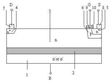
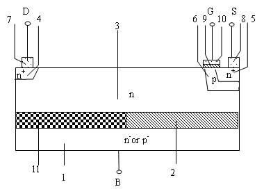
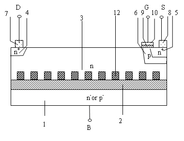
[0037] Figure 7 It is a schematic diagram of an SOI structure with an interface lateral variable doping layer, as shown in the figure: the SOI withstand voltage structure with an interface lateral variable doping provided by the present invention includes a substrate layer 1, a dielectric buried layer 2, and an active semiconductor layer 3, The dielectric buried layer 2 is disposed between the substrate layer 1 and the active semiconductor layer 3, and also includes an interfacial lateral variable doping layer 15, and the interface lateral variable doping layer 15 is disposed between the dielectric buried layer 2 and the active semiconductor layer 3. Between the semico...


PUM

PropertyMeasurementUnit
Thicknessaaaaaaaaaa
Lengthaaaaaaaaaa

Abstract

The invention discloses a silicon on insulator (SOI) pressure resistant structure with interface lateral variation doping, and relates to a semiconductor power device comprising a substrate layer, a medium buried layer, an active semiconductor layer and an interface lateral variation doping layer, wherein, the medium buried layer is arranged between the substrate layer and the active semiconductor layer; and the interface lateral variation doping layer is arranged between the medium buried layer and the active semiconductor layer, in the invention, by adopting the condition that the interface lateral variation doping layer is arranged in the active semiconductor layer on the interface of the medium buried layer, when the structure is used in the semiconductor device, and the dosage concentration of the silicon at the top of the lateral variation doping layer terminal interface is higher, thus effectively improving the longitudinal pressure resistance and the lateral pressure resistance of the device, thus the structure can effectively improve the pressure resistance of the whole device, and remit the problem that a 'hot spot' area is generated because the dosage concentration of a source end of a lateral variation doping structure of the whole active semiconductor layer is too low, which can be realized in a thick active semiconductor layer.

Description

technical field [0001] The invention relates to a semiconductor power device, in particular to a power device with an SOI pressure-resistant structure with lateral variable doping at the interface. Background technique [0002] Silicon on insulator (Semiconductor On Insulator or SOI) is a semiconductor material with a new structure developed rapidly in the 1980s. Its unique structural characteristics overcome the shortcomings of many bulk silicon materials and give full play to the potential of silicon integrated circuit technology. Known as the silicon integration technology of the 21st century, it has received extensive attention and in-depth research from many scholars at home and abroad. [0003] SOI High Voltage Integrated Circuit (High Voltage Integrated Circuit, HVIC) integrates SOI technology, microelectronics technology and power electronics technology, and has become a new branch in the field of power integrated circuits. It has developed rapidly in recent years. ...

Claims


Application Information

Patent Timeline
IPC IPC(8): H01L27/12H01L29/78H01L29/06
Inventor 胡盛东周建林甘平周喜川张玲
Owner CHONGQING UNIV
Why Eureka
Try Eureka