N-type ZnO and p-type GaN combined ZnO-base vertical cavity surface emitting laser and manufacturing method thereof
A technology of vertical cavity surface emission and lasers, which is applied in the direction of lasers, laser components, semiconductor lasers, etc., can solve the problems of low output power of devices, no preparation of controllable resonators, and poor laser directionality, etc., to improve output power , reduce the threshold current, and expand the application range
- Summary
- Abstract
- Description
- Claims
- Application Information
AI Technical Summary
Problems solved by technology
Method used
Image
Examples
Embodiment 1
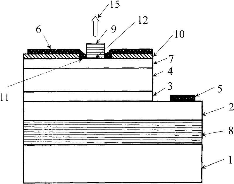
[0033] ZnO-based vertical-cavity surface-emitting laser with upper current confinement window structure n-type ZnO and p-type GaN combination. The ZnO-based vertical cavity surface-emitting laser structure with upper current confinement window structure n-type ZnO and p-type GaN is shown in the appendix image 3 , the preparation method is characterized in that all epitaxial layers of the device are prepared by MOCVD method, with Al 2 o 3 substrate as an example, using the current mature conventional MOCVD preparation method on Al 2 o 3 A multi-layer AlGaN / GaN thin film DBR lower reflector 8 is grown on the substrate, and the central wavelength of its reflection is controlled to be the designed laser lasing wavelength λ, and its reflectivity can be 30% to 99.99%, and then a p-type GaN epitaxial layer 2 is grown, The thickness of the layer is controlled to be one-half λ of N, and N is an odd number, and then the MOCVD method is used, especially the ZnO thin film special-purp...
Embodiment 2
[0035] ZnO-based vertical cavity surface emitting laser combined with n-type ZnO and p-type GaN with internal current confinement window structure. The structure of ZnO-based vertical cavity surface emitting laser combined with n-type ZnO and p-type GaN with internal current confinement window structure is shown in the appendix Figure 4 , the preparation method is characterized in that a silicon dioxide current isolation layer 10 with a thickness of 20-500 nanometers is evaporated on the p-type GaN epitaxial layer 2 with an electron beam evaporation table, and the current limiting window 11 is etched by photolithography, and then Prepare MgO current lower confinement layer 3, n-type ZnO light-emitting layer 4 and MgZnO current upper confinement layer 7 by MOCVD method, the preparation method and thickness requirements are the same as in Example 1; the rest of the epitaxial layers, electrodes and multi-layer dielectric film DBR upper reflector The preparation of 9 is also the ...
Embodiment 3
[0037] Ion implantation bombardment ZnO-based vertical-cavity surface-emitting laser with a current-confined window structure combining n-type ZnO and p-type GaN. The structure of ZnO-based vertical cavity surface-emitting laser combined with n-type ZnO and p-type GaN in this ion implantation bombardment current-limited window structure is shown in the appendix Figure 5 , the preparation method is characterized in that a layer of high-resistance current isolation layer 13 is prepared in the ZnO-based material light-emitting layer 4 by ion implantation bombardment method to form a current confinement window 11; the preparation process is briefly described as follows, on the substrate with The MOCVD method sequentially grows the long multilayer AlGaN / GaN thin film DBR lower mirror 8, the p-type GaN epitaxial layer 2, the current lower confinement layer 3, the n-type ZnO-based material light-emitting layer 4 and the current upper confinement layer 7, and adopts our invented The ...
PUM
 Abstract
Description
Claims
Application Information


