Semiconductor structure and manufacturing method thereof

A manufacturing method and semiconductor technology, applied in the fields of semiconductor/solid-state device manufacturing, semiconductor devices, electrical components, etc., can solve problems such as hindering device performance and low dielectric constant, and achieve the effect of improving performance and reducing EOT

Inactive Publication Date: 2011-09-28
TSINGHUA UNIV
View PDF2 Cites 0 Cited by
  • Summary
  • Abstract
  • Description
  • Claims
  • Application Information

AI Technical Summary

Problems solved by technology

However, a silicon oxide interfacial layer with a thickness of 1nm will be produced between the high-k material and the silicon substrate during the subsequent thermal annealing process, because of its low dielectric constant, which prevents further reduction of EOT and hinders the device Further performance improvements

Method used


Image

  • Semiconductor structure and manufacturing method thereof
  • Semiconductor structure and manufacturing method thereof
  • Semiconductor structure and manufacturing method thereof

Examples


Embodiment 1

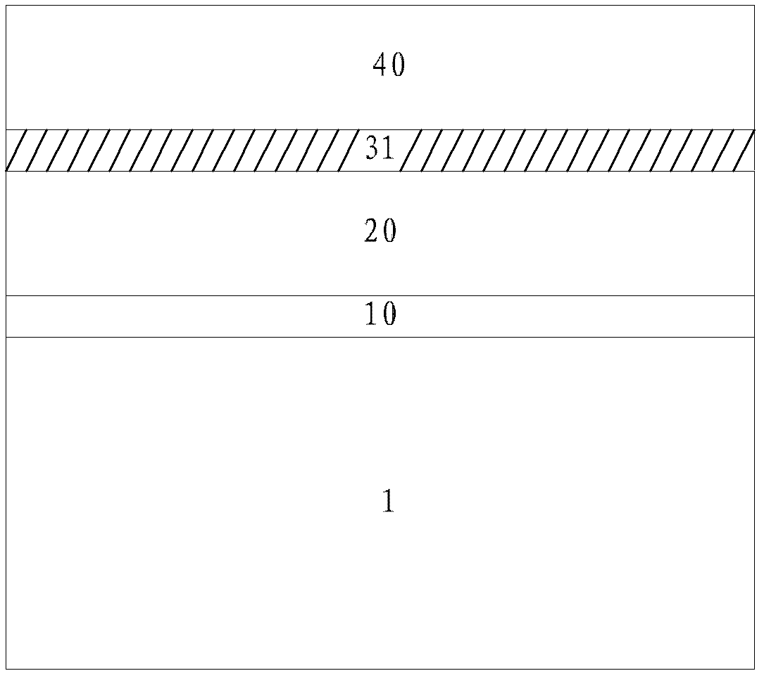
[0031] Such as figure 1 Shown is a schematic diagram of a semiconductor structure according to an embodiment of the present invention. The semiconductor structure includes an interface layer 10 , a gate dielectric layer 20 , an oxygen absorbing layer 31 and a metal gate electrode layer 40 in sequence from the substrate 1 upward. Wherein, the metal atom in the oxygen absorbing layer 31 has a higher ability to bind oxygen than the atoms in the gate dielectric layer 20 and the interface layer 10 below the oxygen absorbing layer 31 .

[0032] In this embodiment, the thickness of the oxygen absorbing layer 31 is set so that the oxygen in the interface layer 10 can be partially adsorbed, or the oxygen in the interface layer 10 can be completely adsorbed, and the specific amount of adsorption needs to be set according to the process conditions. Set and adjust.

[0033] The material of the oxygen absorbing layer 31 includes one or more of metal and metal nitride. Wherein, the dielec...

Embodiment 2

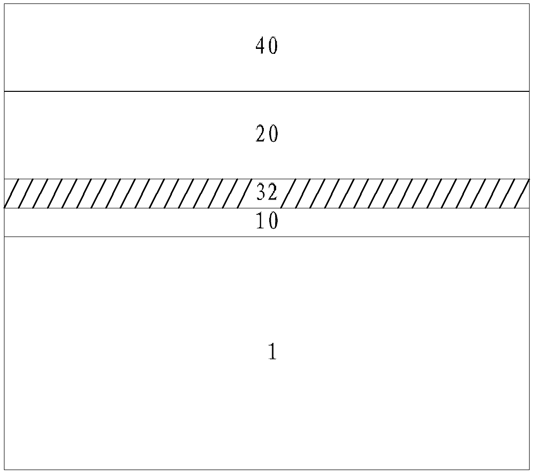
[0037] Such as figure 2 Shown is a schematic diagram of a semiconductor structure according to another embodiment of the present invention. The semiconductor structure includes an interface layer 10 , an oxygen absorbing layer 32 , a gate dielectric layer 20 and a metal gate electrode layer 40 from the substrate 1 to the top.

[0038]The setting of the oxygen absorbing layer 32 in this embodiment is similar to that of Embodiment 1, and will not be repeated here for the sake of simplicity. The difference is that in this embodiment, the oxygen absorbing layer 32 is formed on the interface layer 10, and the absorbing The ability of metal atoms in the oxygen layer 32 to bind oxygen is higher than the ability of atoms in the interface layer 10 below the oxygen absorbing layer 32 to bind oxygen.

[0039] In order to realize Embodiment 2, the present invention also proposes another method for manufacturing a semiconductor structure, comprising the following steps: firstly setting a ...

Embodiment 3

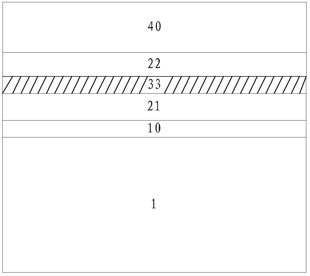
[0041] Such as image 3 Shown is a schematic diagram of a semiconductor structure according to yet another embodiment of the present invention. The semiconductor structure includes: an interface layer 10, a first gate dielectric layer 21, an oxygen absorbing layer 33, a second gate dielectric layer 22 and Metal gate electrode layer 40 .

[0042] The arrangement of the oxygen absorbing layer 30 in this embodiment is similar to that of Embodiment 1 and Embodiment 2, and will not be repeated here for the sake of simplicity. The difference is that in this embodiment, the oxygen absorbing layer 33 is formed on the first gate dielectric layer 21 and the second gate dielectric layer 22, and the metal atoms in the oxygen absorbing layer 33 have a higher binding ability to oxygen than the interface layer 10 below the oxygen absorbing layer 33 and the first gate dielectric layer 21. , that is, the oxygen absorbing layer 33 needs to have a stronger ability to bind oxygen than the first ...


PUM


Abstract

The invention provides a semiconductor structure and a manufacturing method thereof. The semiconductor structure comprises an interface layer positioned on a substrate, a gate medium layer positioned on the interface layer, a metal gate electrode layer positioned on the gate medium layer, and at least one oxygen absorbing layer, wherein the combining capacity of metal atoms and oxygen in the oxygen absorbing layer is higher than the combining capacity of the atoms and oxygen in a laminating material under the oxygen absorbing layer. In the invention, the oxygen in the interface layer is absorbed by adding at least one oxygen absorbing layer, so that the aims of reducing the equivalent oxide layer thickness (EOT) and improving the performance of the device are fulfilled.

Description

technical field [0001] The invention relates to the technical field of integrated circuit manufacturing, in particular to a semiconductor structure and a manufacturing method thereof. Background technique [0002] In the existing CMOS process, in order to improve the performance of the device, a high-k (permittivity) gate dielectric material is usually used instead of the silicon oxide material as the gate dielectric of the CMOS device. The high-k gate dielectric material has a higher dielectric constant than silicon oxide, which can increase the size of the gate capacitance without reducing the physical thickness, thereby reducing the equivalent oxide layer thickness (Equivalent Oxide Thickness, EOT), improve device performance. The further shrinking of the device size requires the EOT to be thinned accordingly. The 2009 ITRS required that the EOT be reduced to 0.5nm in 2016. However, a silicon oxide interfacial layer with a thickness of 1nm will be produced between the h...

Claims


Application Information

Patent Timeline
Patent Type & Authority Applications(China)
IPC IPC(8): H01L29/51H01L29/78H01L21/28H01L21/8238H01L21/265
Inventor 赵梅梁仁荣王敬许军
Owner TSINGHUA UNIV
Why Eureka
Try Eureka