

Tunneling field effect transistor and preparation method thereof
A tunneling field effect and transistor technology, which is applied in semiconductor/solid-state device manufacturing, semiconductor devices, electrical components, etc., can solve problems such as leakage current rise and sacrifice device performance
- Summary
- Abstract
- Description
- Claims
- Application Information
AI Technical Summary
Problems solved by technology
Method used
Image

Examples
Embodiment Construction
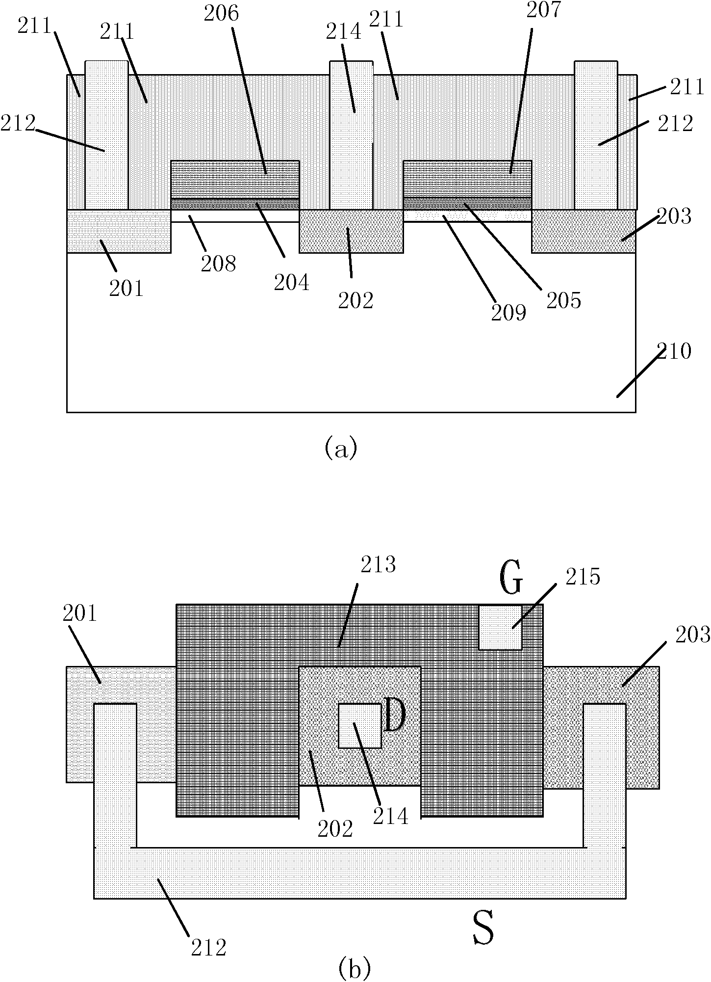
[0098] figure 2 is an embodiment of the first manufacturing method of the Tunneling Field Effect Transistor disclosed in the present invention, wherein figure 2 (a) is a cross-sectional view of the device along the channel length direction, figure 2 (b) is the top view of the device. The device has three electrodes in total: drain electrode D, gate electrode G and source electrode S, which is a three-terminal device. The device includes a first gate stack region, a second gate stack region, a first source region 201 , a second source region 203 , a drain region 202 and a substrate region 210 . Wherein, the first gate stack region includes a first insulating layer 204 and a first conductive layer 206 , and the second gate stack region includes a second insulating layer 205 and a second conductive layer 207 . The insulating film material used for the first insulating layer 204 and the second insulating layer 205 is silicon dioxide obtained by thermal oxidation growth or de...
PUM
 Abstract
Description
Claims
Application Information