Transparent conductive laminated body with visible adjustment layers
A transparent conductive layer, transparent conductive technology, applied to the conductive layer, oxide conductor, non-metallic conductor, etc.
- Summary
- Abstract
- Description
- Claims
- Application Information
AI Technical Summary
Problems solved by technology
Method used
Image
Examples
Embodiment
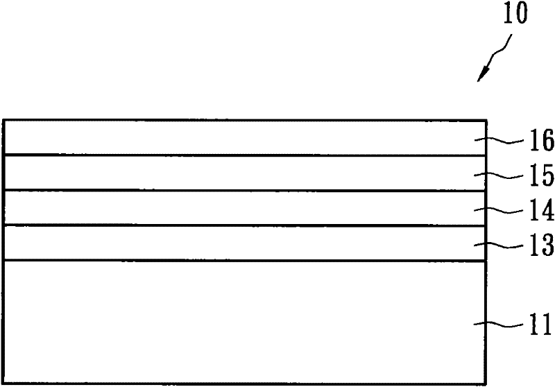
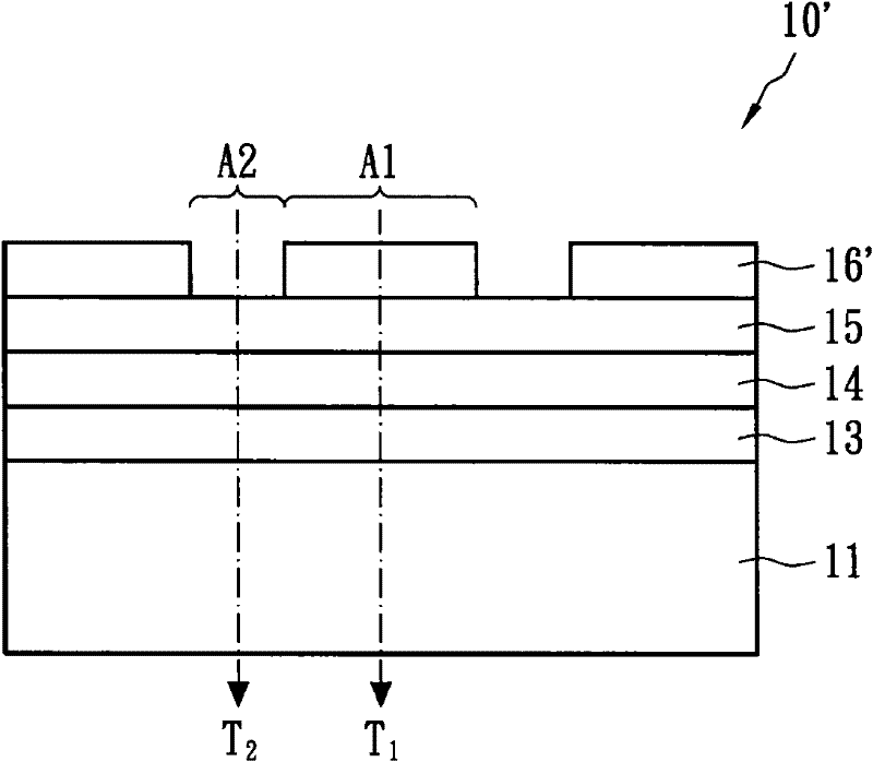
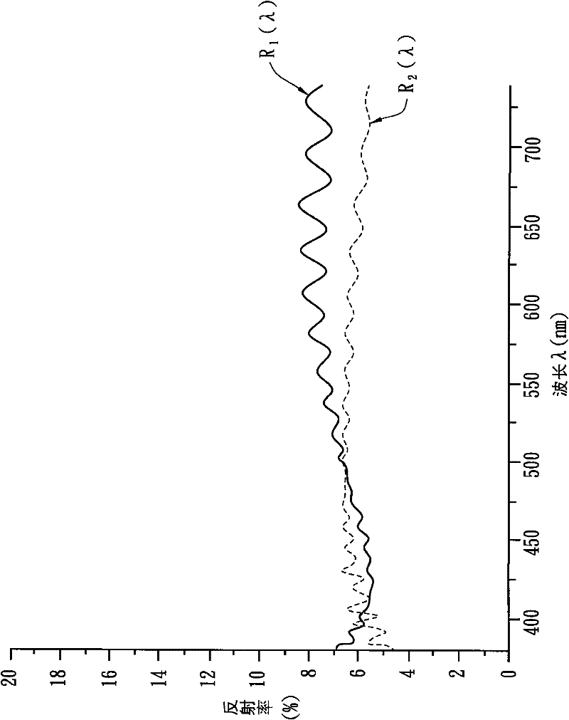
[0051] The embodiment of the present invention discussed below selects a polyethylene terephthalate (PET) substrate with a double-sided hardening treatment, its refractive index is about 1.43, and its thickness is 135 μm. The first visible light adjustment layer is wet-coated. The second visible light adjustment layer, the third visible light adjustment layer, the transparent conductive layer and the intermediate layer are formed by dry sputtering. Wherein the first visible light adjustment layer is Silicon-fluorine (fluorine) copolymer resin, and the second visible light adjustment layer is TiO 2 , the third visible light adjustment layer is SiO 2 , the transparent conductive layer is ITO, and the intermediate layer is SiOx. Comparative example is to select the polyethylene terephthalate (PET) base material that has double-sided hardening treatment, and its refractive index is about 1.43, and thickness is 135 μ m, the first buffer layer, the second buffer layer, and transpar...
PUM
| Property | Measurement | Unit |
|---|---|---|
| Surface resistance | aaaaa | aaaaa |
| Optical thickness | aaaaa | aaaaa |
| Physical thickness | aaaaa | aaaaa |
Abstract
Description
Claims
Application Information


