Device and method for etching conductive film of unviewable zone on touch screen

A conductive film, touch screen technology, applied in welding equipment, laser welding equipment, metal processing equipment, etc., can solve the problems of small tension value, low yield, and environmental impact, and achieve the effect of complete function and linear stability.

Inactive Publication Date: 2011-10-19
SUZHOU DELPHI LASER +1
View PDF5 Cites 5 Cited by
  • Summary
  • Abstract
  • Description
  • Claims
  • Application Information

AI Technical Summary

Problems solved by technology

[0003] The realization of the line function of the traditional conductive film layer is to use the screen printing method. The thinnest printing width of the conductive film material in the invisible area can only reach 100um, and the yield rate is low, the linearity is uneven, and it is cumbersome to replace different batches of products. Cleaning with chemical liquid, the stretching net tension value is small, the cost is also high, the waste gas and liquid produced seriously affect the environment, the finished material has poor wear resistance and chemical resistance, and is easy to age and become brittle
This printing method has complex procedures, requires more consumables in production, and requires more manpower to maintain the production line, which has great limitations. The poor linearity of the conductive film material pins in the invisible area of ​​​​screen printing has become an important cause of failure of displays and touch screens. Factors, these defective products are an important waste of electronic materials that are close to finished products

Method used


Image

  • Device and method for etching conductive film of unviewable zone on touch screen
  • Device and method for etching conductive film of unviewable zone on touch screen
  • Device and method for etching conductive film of unviewable zone on touch screen

Examples


Embodiment Construction

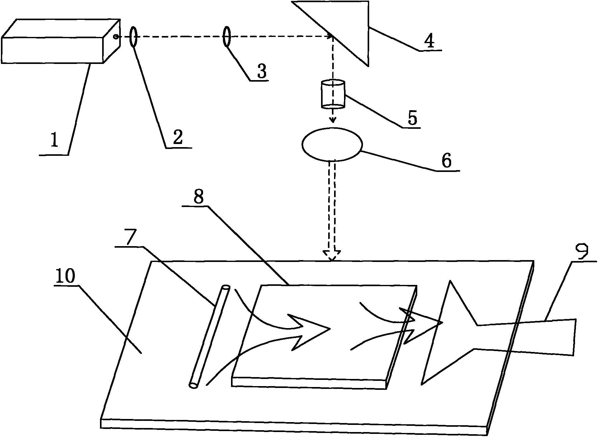
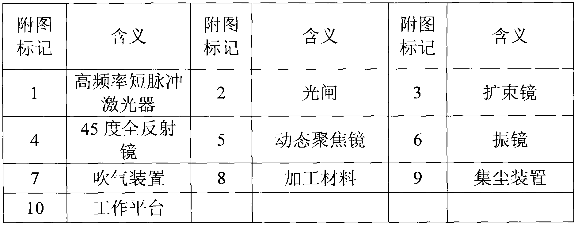
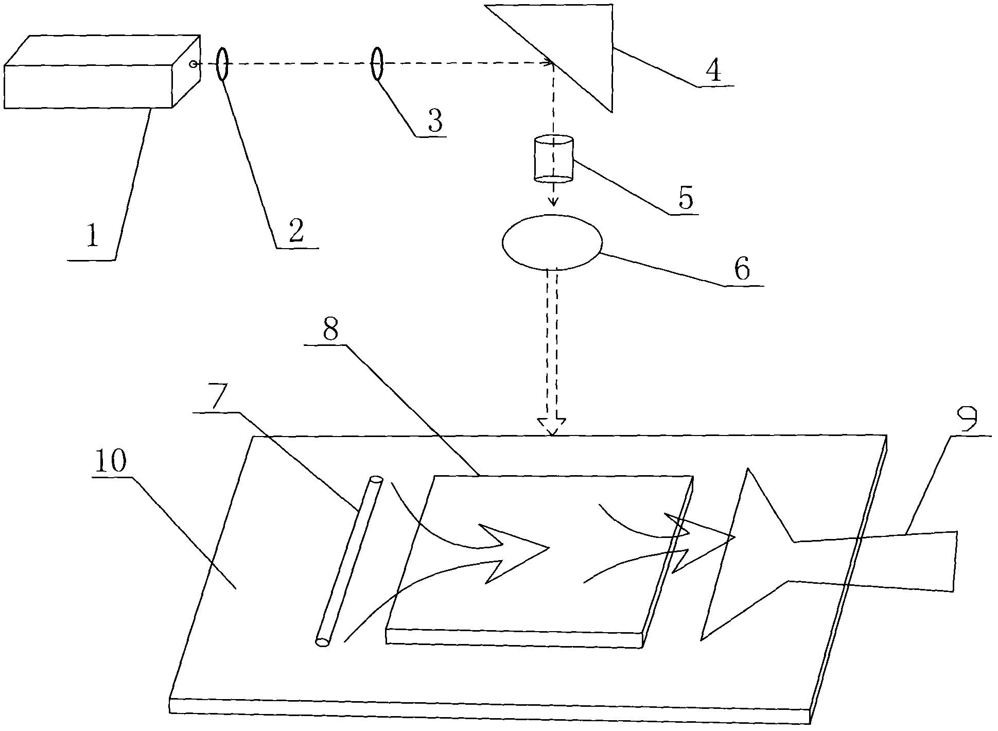
[0016] The invention provides a device and method for laser etching conductive film materials in invisible areas on a touch screen. A high-frequency short-pulse laser is used, and the processed material is a high-conductivity conductive film material. The laser passes through a dynamic focusing mirror and a vibrating mirror. The entire 500mm×500mm invisible area is focused within the range of the conductive film material, and the conductive film material in the invisible area absorbs pulsed laser gasification with high peak power to achieve the etching effect.

[0017] like figure 1 As shown, in the device for etching the conductive thin film in the invisible area on the touch screen, the output end of the high-frequency short-pulse laser 1 is arranged with an optical gate 2. The high-frequency short-pulse laser 1 has a wavelength of 266nm-1064nm and a pulse width of 100ps- For lasers with a frequency of 50 ns and a frequency of 10KHz to 200KHz, the output end of the shutter 2...


PUM

PropertyMeasurementUnit
wavelengthaaaaaaaaaa

Abstract

The invention discloses a device and method for etching a conductive film of an unviewable zone on a touch screen. The output end of a high-frequency short-pulse laser is provided with an optical shutter; the output end of the optical shutter is provided with a beam expander; the output end of the beam expander is successively provided with 45-degree total reflection mirrors; the output end of each 45-degree total reflection mirror is successively provided with a dynamic focus lens and a scanning field lens; the scanning field lens just faces to a working platform; one side of the working platform is provided with a blowing device; and the other side of the working platform is provided with a dust catching plant. The conductive film material of the unviewable zone is etched by an optimized optical path focusing system and a high-frequency pulse laser, thus a thinner and stable line width is obtained, and a substrate is not damaged.

Description

technical field [0001] The invention relates to a laser micromachining device, in particular to a device and method for etching a conductive thin film in an invisible area on a touch screen. Background technique [0002] Due to the continuous growth of demand for electronic products for different purposes such as the IT industry (small cell) and television (large cell), there are higher etching functional requirements for the etching of conductive films on glass substrates or invisible areas of PET substrates. Specifically, when the thickness of the etched conductive film varies within the range of 200nm to 30um, it is possible to produce stable, small line width, and fully functional conductive film layer lines. [0003] The realization of the line function of the traditional conductive film layer is to use the screen printing method. The thinnest printing width of the conductive film material in the invisible area can only reach 100um, and the yield rate is low, the linear...

Claims


Application Information

Patent Timeline
Patent Type & Authority Applications(China)
IPC IPC(8): B23K26/40B23K26/064B23K26/362
Inventor 赵裕兴狄建科张伟
Owner SUZHOU DELPHI LASER
Why Eureka
Try Eureka