

Schottky device with groove structure
A Schottky contact and trench technology, applied in semiconductor devices, electrical components, circuits, etc., can solve the problems of reducing device current density, decreasing forward conduction current, and not improving forward characteristics of devices. It is easy to realize and improve the effect of forward conduction current
- Summary
- Abstract
- Description
- Claims
- Application Information
AI Technical Summary
Problems solved by technology
Method used
Image

Examples
Embodiment Construction
[0014] The present invention is described in more detail below in conjunction with accompanying drawing example:
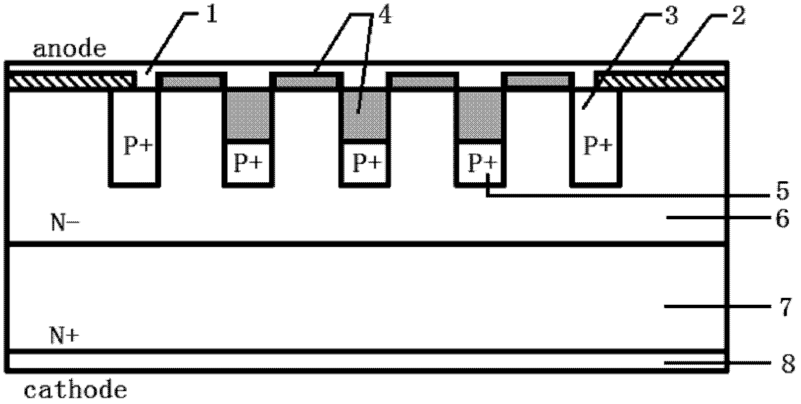
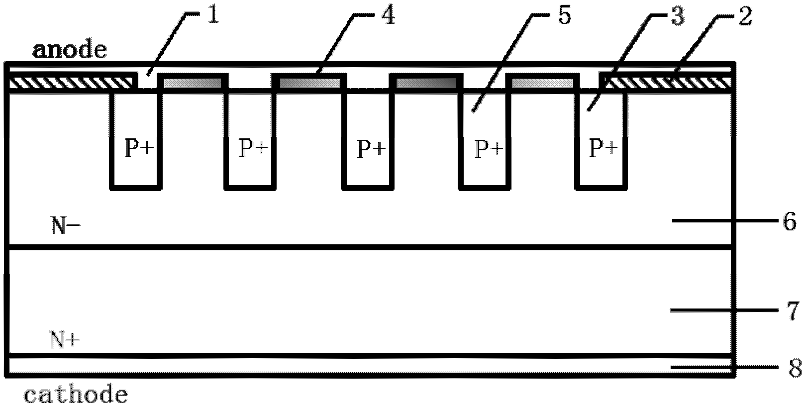
[0015] refer to figure 1 , the trench structure Schottky device of the present invention. It includes an anode electrode 1 , a silicon dioxide layer 2 , a P+ guard ring 3 , a Schottky contact 4 , a P-type doped region 5 , an N-type drift region 6 , an N+ substrate region 7 , and a cathode electrode 8 . According to the requirements of the specific conduction characteristics and breakdown characteristics of the device, determine figure 1 The doping concentration and two-dimensional size of the drift region 6, and the two-dimensional size of the silicon dioxide layer 2. The ratio of the Schottky metal to the P-type doped region in the trench as well as the trench spacing and depth are adjusted according to the requirement for increasing the forward conduction current.
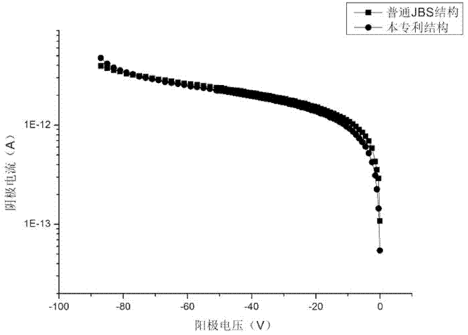
[0016] refer to image 3 , by the comparison of breakdown voltage characteristics of trench...
PUM
 Abstract
Description
Claims
Application Information