Zinc oxide single crystal polishing technology for substrate of photoelectric device

A zinc oxide single crystal, zinc oxide technology, applied in the direction of grinding equipment, grinding machine tools, metal processing equipment, etc.

Inactive Publication Date: 2011-11-16
FUJIAN INST OF RES ON THE STRUCTURE OF MATTER CHINESE ACAD OF SCI
View PDF6 Cites 23 Cited by
  • Summary
  • Abstract
  • Description
  • Claims
  • Application Information

AI Technical Summary

Problems solved by technology

[0003]Sapphire and SiC single crystals are currently the most commonly used substrates for ZnO / GaN thin film epitaxy, however, due to large lattice mismatch and different thermal expansion coefficients, heterogeneous Epitaxial ZnO / GaN-based thin-film optoelectronic devices have a relatively high defect density. It is generally believed that high-concentration defects will introduce non-radiative recombination centers, thereby seriously affecting the luminescence performance of optoelectronic devices.

Method used


Image

  • Zinc oxide single crystal polishing technology for substrate of photoelectric device
  • Zinc oxide single crystal polishing technology for substrate of photoelectric device
  • Zinc oxide single crystal polishing technology for substrate of photoelectric device

Examples


Embodiment Construction

[0033] The specific steps of the zinc oxide single crystal polishing method that can be used for optoelectronic device substrates provided by the present invention are as follows:

[0034] 1) Single crystal rough grinding: use 320~500 Cw sandpaper to artificially grind the surface of the cut zinc oxide single crystal with a thickness of about 1.0 mm, and the surface of the zinc oxide wafer has no saw marks;

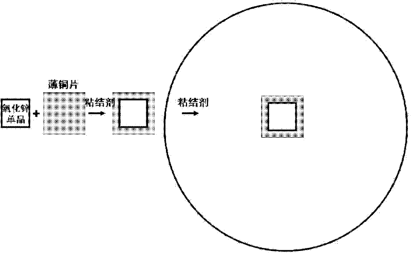
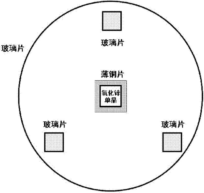
[0035]2) Bonding plate: use 320~500 Cw sandpaper to chamfer the roughly ground zinc oxide wafer with a thickness of about 0.8 mm (see the attached figure 1 ), place the chamfered wafer on the platform of a temperature-controlled / cooled pressurized die bonder for heating, the heating temperature is 80-110 °C, and then use a heated special adhesive to apply it on the upper surface of the wafer while it is hot, and finally Use a cylindrical stainless steel press cake with a diameter of 9 cm to press on the wafer, and the pressure on the wafer is 100~200 g / cm 2 ; After 5 mi...


PUM

PropertyMeasurementUnit
thicknessaaaaaaaaaa
thicknessaaaaaaaaaa
particle sizeaaaaaaaaaa

Abstract

The invention provides a polishing technology of a zinc oxide single crystal substrate, which can meet the requirements for the epitaxial growth of a photoelectric device. The zinc oxide single crystal substrate with the surface RMS (root mean square) roughness of less than 1nm within a surface range of 10 mu m*10 mu m can be obtained through the steps of rough grinding of a single crystal, bonding, loading on a disc, mechanical rough grinding, mechanical fine grinding, mechanical rough polishing, chemical mechanical fine polishing, cleaning and packaging. The polishing technology relates to a bonding agent, a bonding technology and a technology of unloading from the disc used in the bonding process of the zinc oxide single crystal substrate, as well as grinding fluid, polishing fluid and a grinding thickness control technology used in the grinding process and the polishing process. The obtained zinc oxide single crystal substrate can be used for the epitaxial growth of a semiconductor photoelectric device.

Description

technical field [0001] The invention relates to a ZnO single crystal substrate polishing method which can satisfy homoepitaxial / near-mismatched epitaxial growth of semiconductor films. Background technique [0002] Zinc oxide is a direct bandgap II-VI wide bandgap compound semiconductor material, which has excellent characteristics such as large bandgap (3.37 eV), high exciton binding energy (60 meV), and wet chemical etching. It has broad application prospects in optoelectronic devices such as high-efficiency light-emitting diodes (LEDs), laser diodes (LDs), ultraviolet detectors, high-power microwave devices, transparent electrodes, and solar cells. Its application will bring digital storage and detection With the revolution of communication technology, it will completely change the history of human traditional lighting. In addition, ZnO materials also have excellent piezoelectric and gas-sensing properties, and can be used to prepare high-performance acoustic transducers...

Claims


Application Information

Patent Timeline
Patent Type & Authority Applications(China)
IPC IPC(8): B24B37/04
Inventor 林文文黄丰林璋林钟潮黄嘉魁陈达贵陈赛英
Owner FUJIAN INST OF RES ON THE STRUCTURE OF MATTER CHINESE ACAD OF SCI
Why Eureka
Try Eureka