MEMS (micro electro mechanical system) wafer-level three-dimensional mixing integration packaging structure and method

A three-dimensional hybrid, integrated packaging technology, applied in microstructure technology, microstructure devices, manufacturing microstructure devices, etc., can solve the problem of high cost, and achieve the effect of reducing residual stress, simplifying process, and reducing manufacturing cost

Active Publication Date: 2011-11-16
SHANGHAI INST OF MICROSYSTEM & INFORMATION TECH CHINESE ACAD OF SCI
View PDF5 Cites 33 Cited by
  • Summary
  • Abstract
  • Description
  • Claims
  • Application Information

AI Technical Summary

Problems solved by technology

After the wafer-level packaging is completed, it is necessary to further protect the device with the packaging shell. Many famous manufacturers in the world tend to use ceramic shells and QFN (Q

Method used


Image

  • MEMS (micro electro mechanical system) wafer-level three-dimensional mixing integration packaging structure and method
  • MEMS (micro electro mechanical system) wafer-level three-dimensional mixing integration packaging structure and method
  • MEMS (micro electro mechanical system) wafer-level three-dimensional mixing integration packaging structure and method

Examples


Embodiment Construction

[0049] In order to fully demonstrate the advantages and effects of the present invention, the substantive features and remarkable progress of the present invention will be further described below in conjunction with the accompanying drawings and embodiments, but the present invention is not limited by any means.

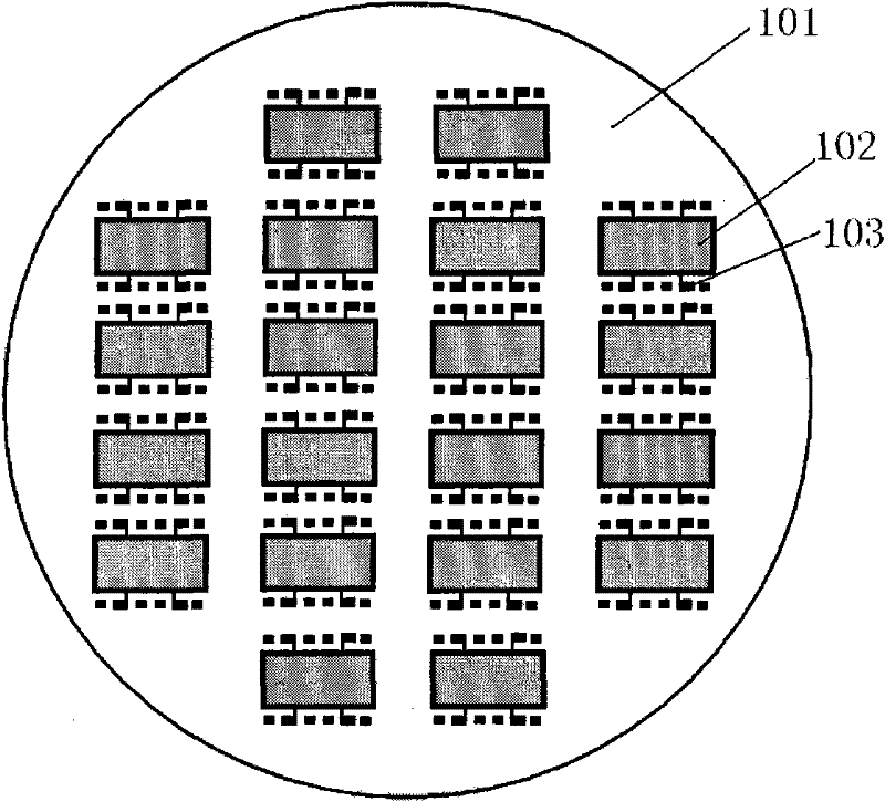
[0050] exist figure 1 Among them, on a silicon wafer 101, 102 is a MEMS device manufactured by MEMS technology, and Al metal leads and pads 103 are electrically connected to the MEMS device.

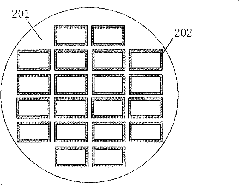
[0051] exist figure 2 Among them, the glass paste sealing ring 202 is printed on the silicon cover wafer 201 by screen printing. The seal ring 202 and the MEMS device 102 correspond to each other.

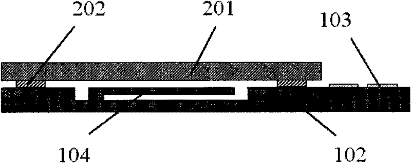
[0052] exist image 3 In the present invention, a silicon wafer 101 with MEMS devices is aligned and bonded to a silicon lid wafer 201 . The Al metal lead and the pad 103 pass through the bonding layer of glass paste to realize the electrical connection of the movable mechanism...


PUM


Abstract

The invention provides an MEMS (micro electro mechanical system) wafer-level three-dimensional mixing integration packaging structure and method based on a Chip to Wafer stacking mode. The method is characterized in that an MEMS device wafer and a silicon cover plate wafer are bonded through low-temperature bonding of glass slurry so as to realize wafer-level airtight/vacuum packaging and finish protection on movable components of the MEMS device; a CMOS (complementary metal oxide semiconductor) chip such as ASIC (application specific integrated circuit) and the like are mounted on and interconnected with the surface of the silicon cover plate wafer in a Chip to Wafer stacking mode so as to realize three-dimensional mixing integration of the CMOS chip such as ASIC and the like and the MEMS device wafer; discrete integrated micro systems are mounted on a low-cost organic substrate; multi-layer interconnection of the CMOS chip, the MEMS device and the substrate is finished through a lead bonding mode; and low-stress plastic package material is filled in a dam mode to protect the integrated micro systems and improve the environment reliability, thus forming an MEMS wafer-level three-dimensional mixing integration packaging structure which has the advantages of high density, low cost, low stress and high reliability and is easy to process.

Description

technical field [0001] The present invention relates to a microelectromechanical system (MEMS) wafer-level three-dimensional hybrid integrated packaging structure and method, more precisely, the present invention relates to a MEMS three-dimensional hybrid integrated packaging method, that is, using Chip to Wafer (chip to wafer A wafer-level three-dimensional hybrid integration method for IC chips and MEMS devices in a laminated manner, which belongs to the field of microsystem packaging. Background technique [0002] Microelectromechanical systems (MEMS) include microsensors and drivers, as well as auxiliary integrated circuits and functional control systems for device function control and signal transmission, conditioning and processing. The integration of MEMS is to package microsensors (or drivers) with CMOS chips such as application-specific integrated circuits (ASICs) and operational amplifier integrated circuits to complete the sensing (or driving) function. At presen...

Claims


Application Information

Patent Timeline
IPC IPC(8): B81B7/00B81C1/00
Inventor 徐高卫罗乐陈骁焦继伟宓斌玮
Owner SHANGHAI INST OF MICROSYSTEM & INFORMATION TECH CHINESE ACAD OF SCI
Why Eureka
Try Eureka