Cu alloy film and display device
A technology for display devices and alloy films, applied in optics, instruments, transistors, etc., can solve problems such as no teaching, and achieve the effects of superior wet etching, low resistivity, and deviation suppression of film thickness distribution
- Summary
- Abstract
- Description
- Claims
- Application Information
AI Technical Summary
Problems solved by technology
Method used
Image
Examples
Embodiment 1-1
[0107] (production of samples)
[0108] In the present embodiment, a pure Cu film or a Cu alloy film (hereinafter, sometimes referred to as a Cu alloy film) is fabricated on a glass substrate (manufactured by Corning Corporation, #1737, diameter 100mm×thickness 0.7mm) by DC magnetron sputtering method. Cu alloy film is a representative) sample (film thickness: 500 nm). The Cu alloy film of this example is composed of a substrate layer and an upper layer (the layer from the substrate layer to the surface of the Cu alloy film), and the oxygen content and alloy composition contained in the substrate layer and the upper layer are shown in Table 1 and Table 2. Among them, sample Nos. 1 to 32 in Table 1 are examples in which the alloy composition (type and content) of the upper layer and the underlayer are the same, and the composition (upper layer=lower layer) column shows the composition of the entire Cu alloy film. For example, in Table 1, No. 5 (upper layer=lower layer=Cu-0.05N...
Embodiment 1-2
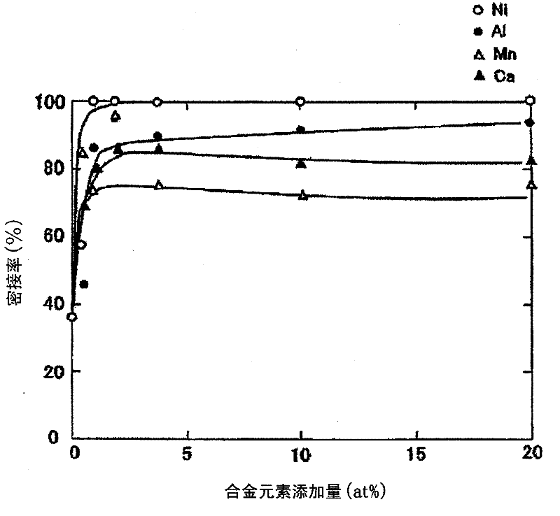
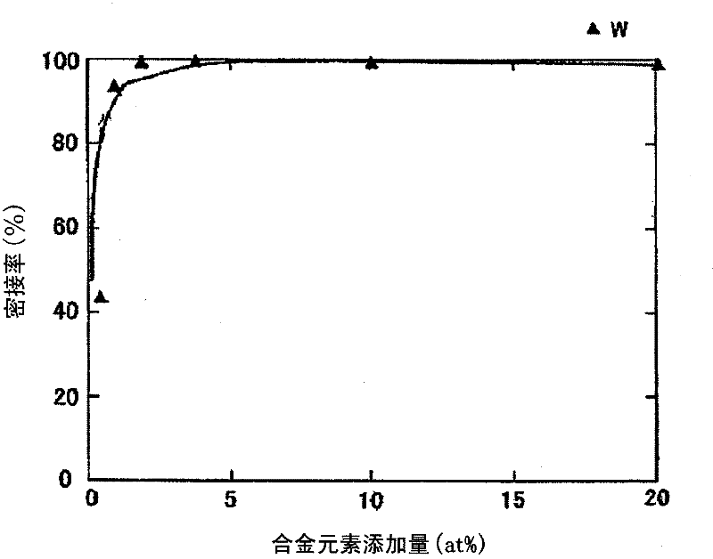
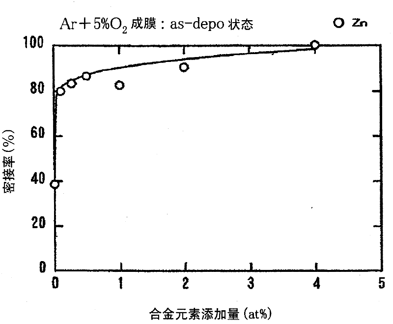
[0163] In this example, the influence of the type and amount of alloy elements in the substrate layer on the adhesion was studied. In this example, as in Example 1-1, a Cu alloy film made of a Cu alloy substrate layer (film thickness: 50nm) and a Cu alloy upper layer (film thickness: 250nm) having the same composition as the substrate layer was produced. material, and a pure Cu film sample with a film thickness of 300 nm for comparison was prepared. The formation of the Cu alloy film is the same as that in Example 1-1, using a sputtering target provided with a chip (chip) containing elements other than Cu (Ni, Al, Mn, W, Zn) on the pure Cu sputtering target. , for Ca, a sputtering target in which a Cu—Ca alloy of a predetermined composition is produced by melting (melting) is used. In addition, adding oxygen to the Cu alloy film is performed by controlling the sputtering gas used in the above-mentioned film formation. More specifically, in the film formation of the substrate...
Embodiment 1-3
[0167] In this example, the influence of the film thickness of the base layer on the adhesion was studied. The preparation of the sample was the same as in Example 1-2 except for the following points. The difference is that both the base layer and the upper layer were made of Cu-2 atomic % Zn, and the film thickness of the base layer was set within the range of 10 to 200 nm. Variety. In addition, as a comparison, a sample in which pure Ar gas was also used in the film formation of the underlayer and the underlayer did not contain the sample was produced. Thereafter, about the sample immediately after film formation, the adhesiveness was evaluated in the same manner as in Example 1-1. The result is as Figure 7 shown.
[0168] according to Figure 7 It can be seen that the adhesiveness tends to improve as the film thickness of the base layer increases. In addition, the effect of improving the adhesion is saturated when the film thickness is about 100 nm, and even if the fi...
PUM
| Property | Measurement | Unit |
|---|---|---|
| electrical resistivity | aaaaa | aaaaa |
| electrical resistivity | aaaaa | aaaaa |
| thickness | aaaaa | aaaaa |
Abstract
Description
Claims
Application Information
 - R&D
- Intellectual Property
- Life Sciences
- Materials
- Tech Scout
- Unparalleled Data Quality
- Higher Quality Content
- 60% Fewer Hallucinations
Browse by: Latest US Patents, China's latest patents, Technical Efficacy Thesaurus, Application Domain, Technology Topic, Popular Technical Reports.
© 2025 PatSnap. All rights reserved.Legal|Privacy policy|Modern Slavery Act Transparency Statement|Sitemap|About US| Contact US: help@patsnap.com


