

Fabrication method of semiconductor structure
A manufacturing method, semiconductor technology, applied in the direction of semiconductor/solid-state device manufacturing, semiconductor devices, semiconductor/solid-state device components, etc., can solve the problems of consumption, time and production costs, etc., to save time and cost, reduce photolithography The number of times, the effect of guaranteed performance
- Summary
- Abstract
- Description
- Claims
- Application Information
AI Technical Summary
Problems solved by technology
Method used
Image

Examples
Embodiment Construction
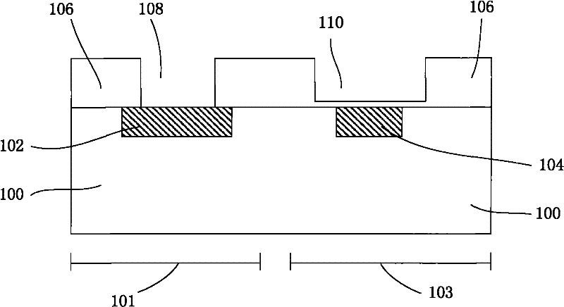
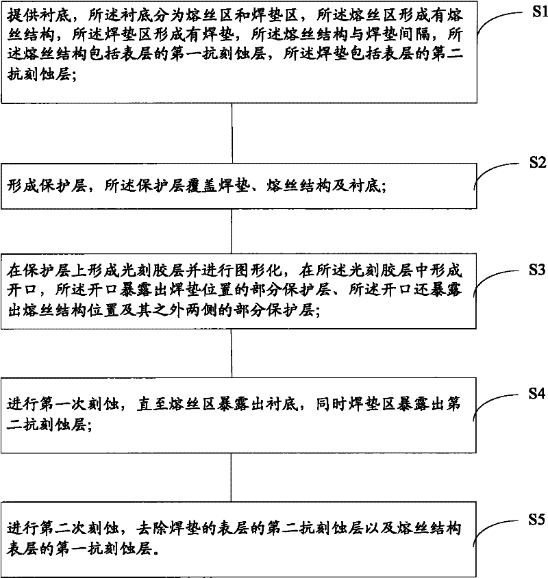
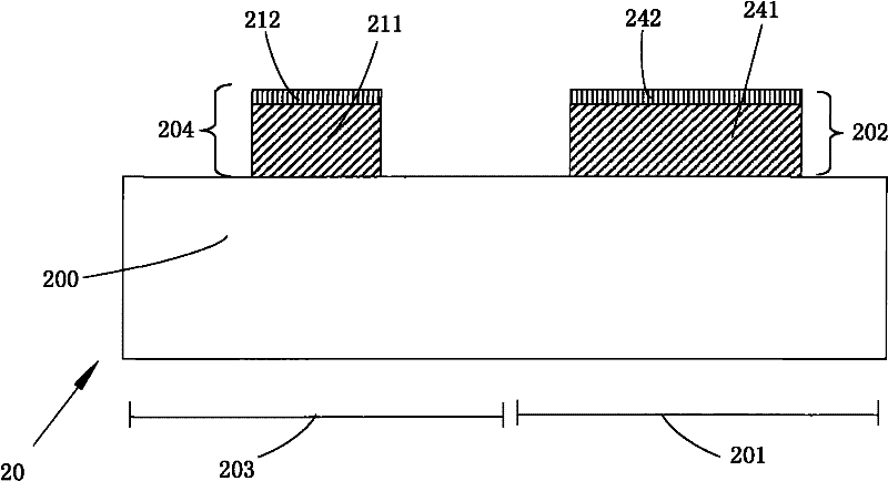
[0028] During the formation of the pad and fuse structure, in order to improve the reliability of the device, two photolithography and etching processes are usually required, one is to protect the fuse area with photoresist, and the protective layer in the pad area Openings are formed in the middle to expose the pads, and then the photoresist in the fuse area is stripped; the other time is to protect the pad area with photoresist, form an opening in the protective layer of the fuse area, and leave a part of the protective layer on the The fuse structure is used for subsequent laser repair, and then the photoresist in the pad area is stripped. Since photolithography needs to be carried out twice and two photomasks are used, more time and production costs are consumed.
[0029] In view of the problems referred to above, the present invention forms the pattern of welding pad and fuse structure simultaneously on the same mask plate after spin-coating photoresist layer on protectiv...
PUM
 Abstract
Description
Claims
Application Information