
Transparent conductive laminate and transparent touch panel using the same

A technology of transparent conductivity and transparent conductive layer, which is applied to the conductive layer on the insulating carrier, the parts of the color TV, the parts of the TV system, etc., and can solve the problem of damage to the transparent conductive layer of the movable electrode substrate, flying debris, display Problems such as poor visibility, achieve wide-angle and image clarity, reduce the frequency of replacement, and achieve the effect of large image clarity

Active Publication Date: 2011-11-30
TEIJIN LTD +1
View PDF9 Cites 10 Cited by
  • Summary
  • Abstract
  • Description
  • Claims
  • Application Information

AI Technical Summary

Problems solved by technology

However, the anti-Newton ring layer formed by this method has the following problems, that is, when the sliding durability and edge pressing durability test required for the touch panel are performed, the transparent conductive layer starts to deteriorate from the protrusions formed by these inorganic particles. Peeling, eventually deteriorating as the electrical characteristics of the touch panel
[0007] In addition, during the dot durability test, the protrusions formed by the inorganic particles contained in the transparent conductive layer forming surface of the movable electrode substrate will destroy the dot spacers formed on the fixed electrode substrate, and the fragments will be scattered in the touch panel.
There is a problem that the dot spacer fragments scattered in this way prevent the connection between the movable electrode substrate and the fixed electrode substrate, deteriorating the electrical characteristics of the touch panel.
In addition, there is also a problem that the fragments of these scattered dot spacers damage the transparent conductive layers of the movable electrode substrate and the fixed electrode substrate, deteriorating the electrical characteristics of the touch panel.
[0008] In addition, when the anti-Newton ring layer formed using such inorganic particles is used as a fixed electrode substrate, there is also a problem that the protrusions formed by the inorganic particles damage the transparent conductive layer of the movable electrode substrate and degrade the electrical characteristics of the touch panel.
In addition, when wet coating using a gravure coater or the like is used to form a resin layer containing fine particles of about several μm, since the fine particles in the coating liquid settle over time, it is necessary to frequently replace the coating liquid. There is a problem with productivity
[0009] As a method for forming irregularities on the surface of the film without using inorganic fine particles of 1 μm or more, there is a compound that can be polymerized by irradiating active energy rays with a thermoplastic resin and inorganic fine particles having an average primary particle diameter of 0.001 μm or more and less than 1 μm or An example of its combination of oligomers, but the layer formed by this method has a problem of poor visibility of the display due to extremely high haze (refer to Japanese Patent Laid-Open No. 2002-275391)

Method used

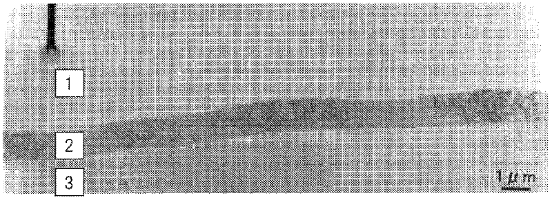
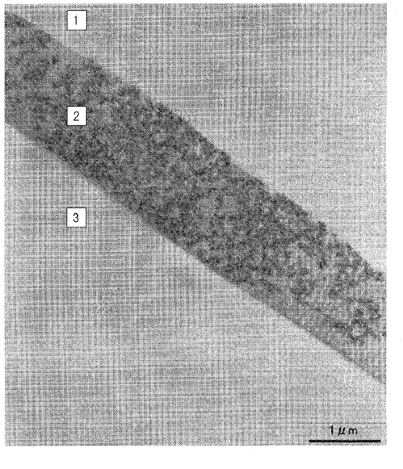

Image

  • Transparent conductive laminate and transparent touch panel using the same
  • Transparent conductive laminate and transparent touch panel using the same
  • Transparent conductive laminate and transparent touch panel using the same

Examples


Embodiment

[0162] Hereinafter, examples are given to illustrate the present invention in more detail, but the present invention is not limited by these examples. It should be noted that, in the Examples, "parts" and "%" are mass references unless otherwise specified. In addition, various measurements in Examples were performed as follows.

[0163]

[0164] The measurement was performed using a probe-type height difference meter DEKTAK3 manufactured by Sloan Company. Measurement was performed in accordance with JIS B0601-1994 edition.

[0165]

[0166] Measurement was performed using Surfcorder SE-3400 manufactured by Kosaka Laboratories. Measurement was performed in accordance with JIS B0601-1982 edition.

[0167]

[0168] The measurement was performed using a stylus type film thickness meter Alphastec manufactured by Anritsu Electric Co., Ltd.

[0169]

[0170] The measurement was performed using a haze meter (MDH2000) manufactured by Nippon Denshoku Co., Ltd.

[0171]

...

Embodiment A and comparative example A

[0182] It will be shown below that by mixing metal oxide ultrafine particles and metal fluoride ultrafine particles in a specific ratio, a weak association state is formed in the cured resin layer, thereby forming a desired concavo-convex shape.

Embodiment A1

[0184] Using a polycarbonate film (manufactured by Teijin Chemicals Co., Ltd., C110-100) (PC) as a transparent organic polymer substrate, a coating liquid R having the following composition was applied on one side with a ring bar coater A , after heating and drying at 40°C for 1 minute, irradiate with a UV lamp at 120mW / cm 2 、400mJ / cm 2 UV rays form a cured resin layer with a film thickness of about 1.5 μm and a concave-convex surface.

[0185] Coating solution R A composition of

[0186] Quadrifunctional acrylate: 100 parts by mass of "ARONIX" M-405 (manufactured by Toagosei Co., Ltd.)

[0187] Metal oxide ultrafine particle dispersion: 80 parts by mass (8 parts by mass in terms of solid content, SiO manufactured by CI Chemicals Co., Ltd. 2 10% by mass isopropanol dispersion of ultrafine particles, primary average particle size of ultrafine particles is 30nm)

[0188] Metal fluoride ultrafine particle dispersion: 20 parts by mass (4 parts by mass in terms of solid conten...


PUM

PropertyMeasurementUnit
particle diameteraaaaaaaaaa
roughnessaaaaaaaaaa
roughnessaaaaaaaaaa

Abstract

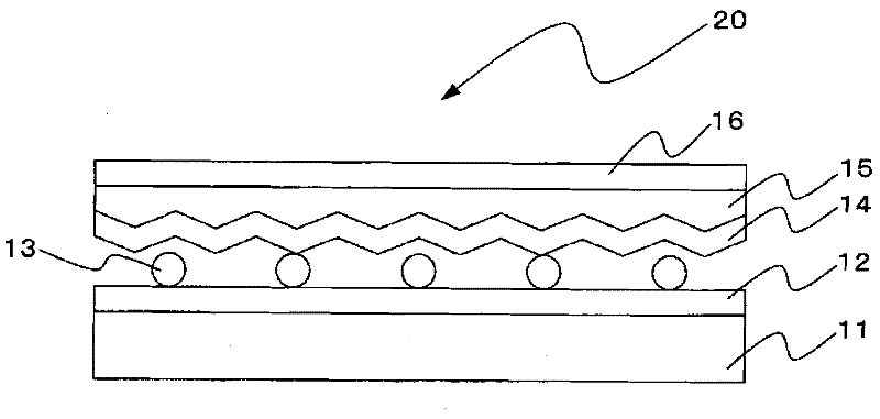
Provided is a transparent electroconductive laminate which can prevent the occurrence of Newton rings between two transparent electrode substrates constituting a transparent touch panel. Also provided is a transparent touch panel which comprises the transparent electroconductive laminate. A transparent electroconductive laminate (14, 15, 16) comprises a transparent organic polymer substrate (16), and comprises an uneven-surfaced hardened resin layer (15) and a transparent electroconductive layer (14) which are successively laminated on at least one side of the transparent organic polymer substrate. The transparent electroconductive laminate is characterized in that the hardened resin layer comprises a hardening resin component and at least one of ultrafine metal oxide particles (A) and ultrafine metal fluoride particles (B), these particles having an average primary particle diameter of 100 nm or less and being dispersed in the hardening resin component. The contents of the ultrafine particles (A) and (B) in the hardened resin layer are each 1 part by mass or more to less than 20 parts by mass per 100 parts by mass of the hardening resin component. The ratio by mass (A / B) of the ultrafine particles (A) to the ultrafine particles (B) is greater than 0.3. A transparent touch panel (20) comprises the aforesaid transparent electroconductive laminate (14, 15, 16).

Description

technical field [0001] The present invention relates to a transparent touch panel and a transparent conductive laminate suitable therefor. More specifically, the present invention relates to a transparent touch panel excellent in visibility and a transparent conductive laminate used therefor. Background technique [0002] In recent years, transparent touch panels that realize interactive input methods as one of man machine interfaces have been widely used. The transparent touch panel includes an optical method, an ultrasonic method, an electrostatic capacitance method, a resistive film method, etc. according to a position detection method. Among them, the resistive film method has seen rapid popularity in recent years because of its simple structure and good price / performance ratio. [0003] The transparent touch panel of the resistive film method is an electronic component composed of two films or sheets with a transparent conductive layer on the opposite side. The movabl...

Claims


Application Information

Patent Timeline
Patent Type & Authority Applications(China)
IPC IPC(8): H01B5/14B32B7/02B32B9/00B32B27/20C23C14/08G06F3/041H04N5/72C08J7/044C08J7/046
CPCC23C14/086C08J7/04C08J2433/06C08J2369/00G06F3/045C08J2367/02G02B6/0051G02F1/13G06F3/047B32B11/02C08J7/045Y10T428/24364C08J7/0423C08J7/046C08J7/044G06F3/0412G06F2203/04113H01B5/14
Inventor 伊藤晴彦今村公一
Owner TEIJIN LTD
Learn More