nanoimprint method

A technology of nanoimprinting and embossing machine, which is applied in nanotechnology, nanotechnology, nanotechnology for information processing, etc., and can solve the problem of reduced mechanical stability of nanoimprinting resist, unfavorable application, and template pretreatment process Complicated problems, to achieve the effect of ensuring integrity and resolution, ensuring resolution and fidelity, and reducing defects

Inactive Publication Date: 2011-12-14
TSINGHUA UNIV +1
View PDF4 Cites 7 Cited by
  • Summary
  • Abstract
  • Description
  • Claims
  • Application Information

AI Technical Summary

Problems solved by technology

However, due to the high glass transition temperature of polymethyl methacrylate, the heating temperature in this method is too high, so that the mechanical stability of the nanoimprint resist is reduced, and the adhesion to the template is strong, making it difficult to Demoulding, the obtained pattern is not smooth, so that the resolution of the obtained nano pattern is low
In the prior art, in order to improve the resolution of nanopatterns, it is often necessary to pretreat the template before imprinting, but the pretreatment process of the template is complicated, thus increasing the process complexity and cost of nanoimprinting. This method not conducive to practical application

Method used


Image

  • nanoimprint method
  • nanoimprint method
  • nanoimprint method

Examples


no. 1 example

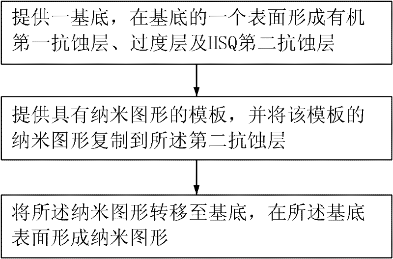
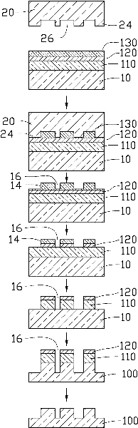
[0028] see figure 1 and figure 2 , using the first embodiment of the nanoimprint method provided by the present invention, which includes the following steps:

[0029] In step S11 , a substrate 10 is provided, and a first resist layer 110 , a transition layer 120 and a second resist layer 130 are sequentially formed on a surface (not shown) of the substrate 10 .

[0030] Firstly, the first resist layer 110 is formed on the surface of the substrate 10 .

[0031] A substrate 10 is provided, and the substrate 10 is cleaned; an organic resist is deposited on a surface of the substrate 10 and then dried to form the first resist layer 110 . The organic resist can be deposited on the substrate 10 by screen printing or spin coating to form the first resist layer 110 . In this embodiment, the organic resist is positive resist ZEP520.

[0032] The material of the base 10 can be a hard material, such as silicon, silicon dioxide, silicon nitride or gallium nitride, and the material o...

no. 2 example

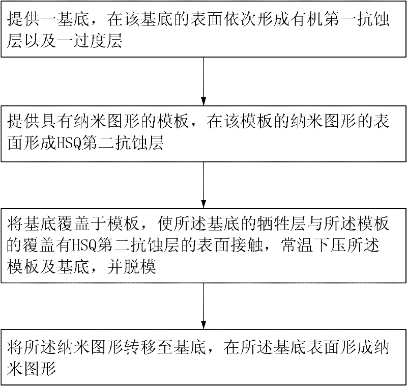
[0053] see image 3 and Figure 4 , the second embodiment of the nanoimprint method using the nanoimprint anti-decoration agent of the present invention, which includes the following steps:

[0054] In step S21 , a substrate 30 is provided, and a first resist layer 310 and a transition layer 320 are sequentially formed on the surface of the substrate 30 .

[0055] In this embodiment, the material of the substrate 30 is completely the same as that of the substrate 10 in the first embodiment, and the manufacturing method, structure, material and positional relationship of the first resist layer 310 and the transition layer 320 are respectively the same as those in the first embodiment. The manufacturing method, structure, material and positional relationship of the first resist layer 110 and the transition layer 120 are completely the same.

[0056] Step S22 , providing a template 60 with nanopatterns on the surface, and forming a second resist layer 330 on the surface of the ...


PUM

PropertyMeasurementUnit
thicknessaaaaaaaaaa
thicknessaaaaaaaaaa
thicknessaaaaaaaaaa

Abstract

A nanoimprint method is provided. A substrate and a master stamp are first provided. The substrate has a first resist layer, a transition layer, and a second resist layer orderly formed thereon. The master stamp has a nanopattern defined therein. The second resist layer is a layer of hydrogen silsesquioxane. The nanopattern of the master stamp is then pressed into the second resist layer to form a nanopattern in the second resist layer at normal temperature which is in a range from about 20 centidegrees to about 50 centidegrees. Finally, the nanopattern of the second resist layer is transferred to the substrate.

Description

technical field [0001] The invention relates to a nanoimprint method, in particular to a nanoimprint method that can be performed at room temperature. Background technique [0002] In the prior art, when making various semiconductor devices, it is often necessary to make nanopatterns with fine structures ranging from tens of nanometers to hundreds of nanometers. The fabrication method of the nano-pattern with the above-mentioned fine structure mainly includes the lithography method of light or electron beam: first, use radiation or electron beam focused through a mask or scanning to irradiate the photoresist composition or mask, the above-mentioned Radiation or electron beams will change the chemical structure of the resist in the exposed area; then, the resist in the exposed area or outside the exposed area is removed by etching to obtain a specific pattern. [0003] In order to adapt to the rapid development of integrated circuit technology, while the existing optical lit...

Claims


Application Information

Patent Timeline
Patent Type & Authority Applications(China)
IPC IPC(8): G03F7/00
CPCG03F7/0002B82Y40/00B82Y10/00
Inventor 朱振东李群庆张立辉陈墨金元浩
Owner TSINGHUA UNIV
Why Eureka
Try Eureka