Composite integrated sensor structure and manufacturing method thereof

A technology integrating sensors and manufacturing methods, applied in the direction of microstructure technology, microstructure devices, manufacturing microstructure devices, etc., can solve the problems of increasing production costs and incompatibility

Active Publication Date: 2011-12-21
ADVANCED SEMICON MFG CO LTD
View PDF8 Cites 14 Cited by
  • Summary
  • Abstract
  • Description
  • Claims
  • Application Information

AI Technical Summary

Problems solved by technology

These processes are the current mainstream, but they are not compatible with conventional semiconductor processes. Therefore, customized sensor processing production lines are required, which increases production costs.

Method used


Image

  • Composite integrated sensor structure and manufacturing method thereof
  • Composite integrated sensor structure and manufacturing method thereof
  • Composite integrated sensor structure and manufacturing method thereof

Examples


Embodiment Construction

[0046] The present invention will be further described below in conjunction with specific embodiment and accompanying drawing, set forth more details in the following description so as to fully understand the present invention, but the present invention can obviously be implemented in a variety of other ways different from this description, Those skilled in the art can make similar promotions and deductions based on actual application situations without violating the connotation of the present invention, so the content of this specific embodiment should not limit the protection scope of the present invention.

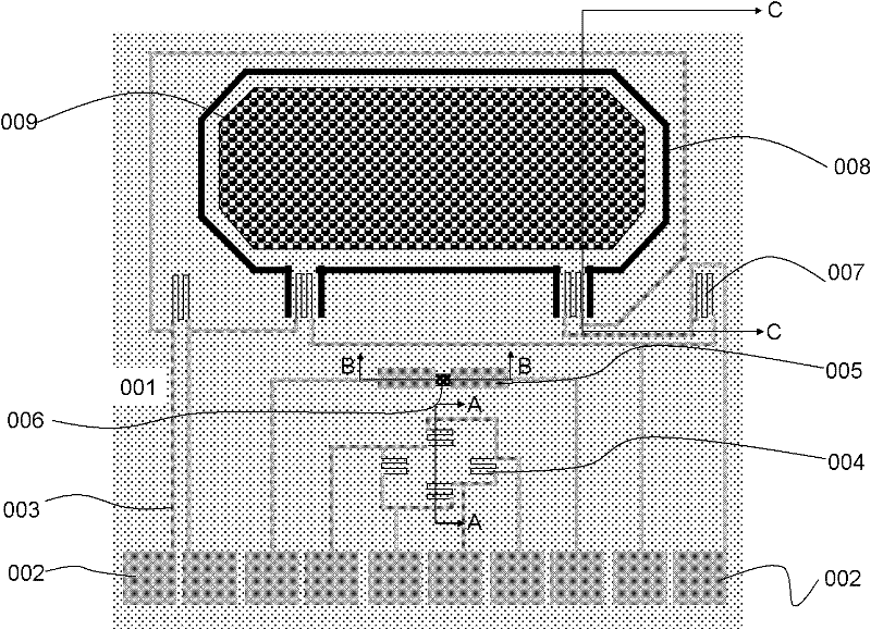
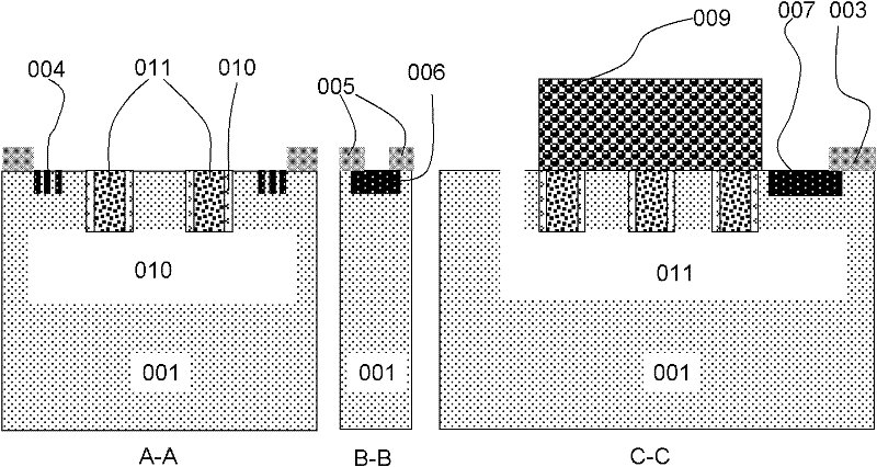
[0047] figure 1 It is a schematic plan view of the composite integrated sensor structure of an embodiment of the present invention. As shown in the figure, it can be seen that the composite integrated sensor structure includes an acceleration sensor (located in the upper half of the figure), a temperature resistance sensor (located in the middle of the figure) and a pre...


PUM


Abstract

The invention provides a manufacturing method of a composite integrated sensor structure. The method comprises the following steps of: providing a substrate and forming a doped region on the substrate; etching the substrate to form a trench for manufacturing a cavity; depositing a barrier layer on the surface of the substrate and the side wall and the bottom of the trench; removing the barrier layers on the surface of the substrate and the bottom of the trench and forming a side wall protection layer on the side wall of the trench; continuously etching the trench under combined action of a hard mask on the substrate and the side wall protection layer to form a deep trench; corroding the deep trench and forming the cavity in the substrate; filling an isolating material and / or a filling material between the side wall protection layers of the trench to form a plug structure to isolate the cavity from the exterior; planarizing the surface of the substrate; manufacturing a conductive lead and an electrode on the surface of the substrate; depositing a mass block at the region of an acceleration sensor and patterning the mass block; and forming an isolating trench around the mass block and connecting the mass block with the substrate in a cantilever mode. In the invention, a front process which is compatible with the conventional semiconductor process is adopted; and the manufacturing method has the advantages of practicability, economy, high performance and the like.

Description

technical field [0001] The invention relates to the technical field of micro-electromechanical systems (MEMS) manufacturing, in particular, the invention relates to a composite integrated sensor structure integrating a temperature sensor, an acceleration sensor and a pressure sensor and a manufacturing method thereof. Background technique [0002] With the development of sensor technology, the sensor chip no longer contains a single sensor device, but appears more in the form of a system on chip (SOC or SIP). In a system-on-chip, multiple sensor device units are often integrated, and even peripheral CMOS integrated circuits are included to form a systematic on-chip composite integrated sensor structure. The appearance of the on-chip sensing system makes the integration of the sensor higher and higher, the function stronger and smaller, and the cost is significantly reduced at the same time. [0003] The structure and manufacturing method of composite integrated sensors are ...

Claims


Application Information

Patent Timeline
Patent Type & Authority Applications(China)
IPC IPC(8): B81C1/00G01D21/02
CPCG01D21/02B81C1/00B81C1/00182
Inventor 张挺谢志峰邵凯
Owner ADVANCED SEMICON MFG CO LTD
Why Eureka
Try Eureka