

A kind of ingot casting method of 800 kg single polycrystalline silicon
A single-polysilicon, kilogram-level technology, applied in the field of crystalline silicon ingots and photovoltaics, can solve problems such as low production capacity, and achieve the effect of large production capacity and advanced technology
- Summary
- Abstract
- Description
- Claims
- Application Information
AI Technical Summary
Problems solved by technology
Method used
Image

Examples
Embodiment Construction
[0034] The present invention will be further described in detail below in conjunction with the accompanying drawings, so that those skilled in the art can implement it with reference to the description.
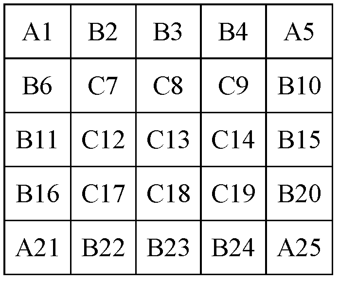
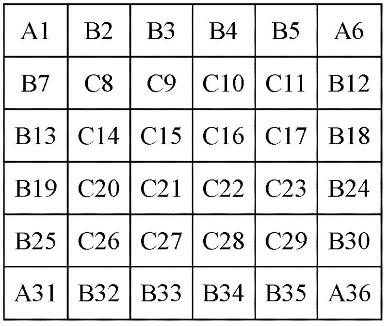
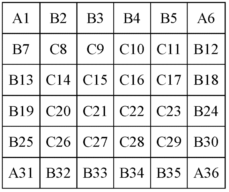
[0035] Such as figure 1 and figure 2 As shown, the present invention provides a method for casting an 800-kilogram single polycrystalline silicon ingot, comprising the following steps:
[0036] Step 1. Select a square monocrystalline silicon wafer with a thickness of 1-50mm and a length and width of 156x156mm, and lay it tightly and evenly on the bottom of the crucible with an outer size of 1050x1050mm;
[0037] Step 2. Add raw polysilicon material and an alloy matched according to the target resistivity on the square monocrystalline silicon wafer, and charge at least 800kg in total;
[0038] Step 3. Vacuuming and leak detection steps: put the crucible containing the above-mentioned silicon material and alloy into the ingot casting furnace, and start pumping and leak detec...
PUM
 Abstract
Description
Claims
Application Information