Semiconductor chip and manufacturing method thereof

A manufacturing method, semiconductor technology, applied in semiconductor/solid-state device manufacturing, semiconductor devices, semiconductor/solid-state device components, etc., can solve problems such as stress generation, reliability impact, high leakage current, etc.

Active Publication Date: 2012-01-11
TAIWAN SEMICON MFG CO LTD
View PDF6 Cites 28 Cited by
  • Summary
  • Abstract
  • Description
  • Claims
  • Application Information

AI Technical Summary

Problems solved by technology

However, the UBM layer may be eroded laterally during the etching process, resulting in an undercut of the UBM layer.
Undercutting of the UBM layer can cause stress during the solder bumping process
Such stress may cause cracking of the low-k dielectric layer in the underlying substrate
In the

Method used


Image

  • Semiconductor chip and manufacturing method thereof
  • Semiconductor chip and manufacturing method thereof
  • Semiconductor chip and manufacturing method thereof

Examples


Embodiment Construction

[0028] The fabrication and discussion of various embodiments of the present invention are discussed in detail below. However, it should be noted that these embodiments provided in the present invention only provide the inventive concept of the present invention, which can be applied in a broad form to various specific cases. The embodiments discussed herein are for illustration only, and do not limit the present invention in various forms.

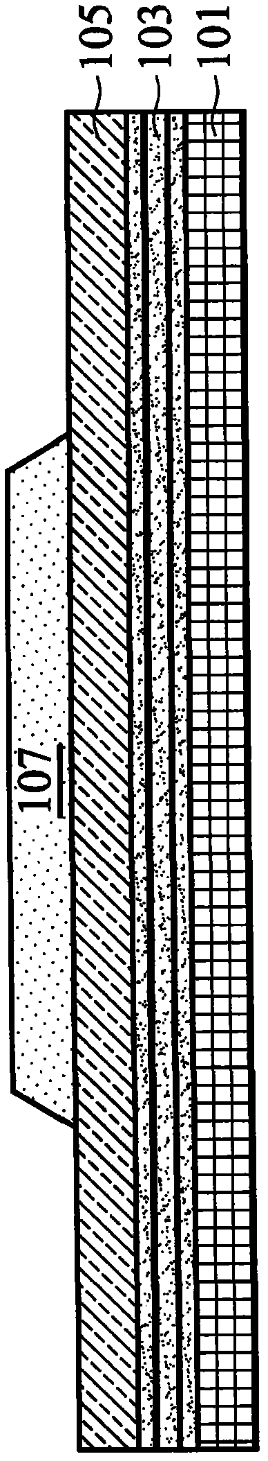
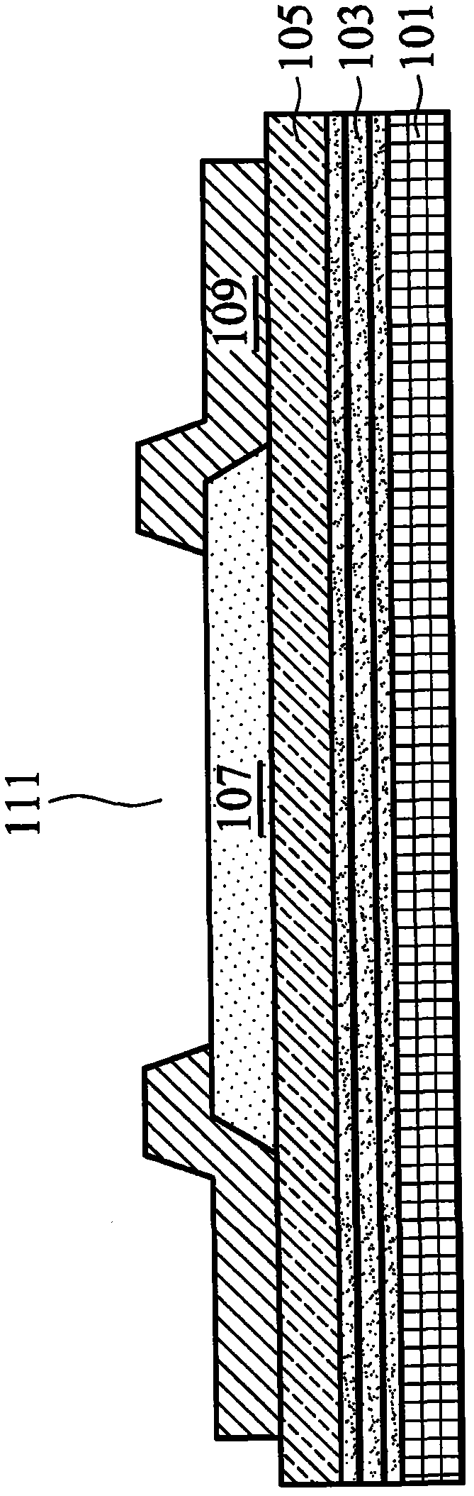
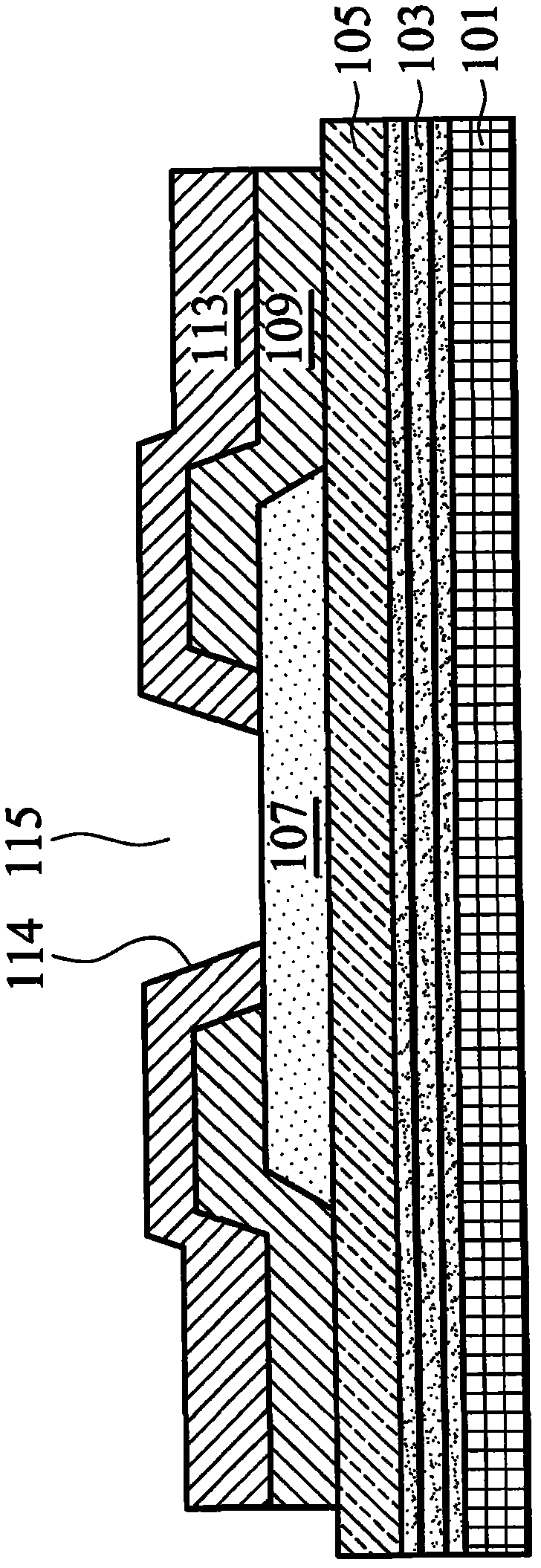
[0029] Figure 1 to Figure 14 Cross-sectional views of structures at various stages of fabrication are shown in accordance with one or more embodiments of the invention. The term "substrate" as used herein refers to a semiconductor substrate on which various film layers and integrated circuit elements are formed. The substrate may comprise silicon or a compound semiconductor such as gallium arsenide, indium phosphide, silicon / germanium or silicon carbide. In some embodiments, layers may include dielectric layers, doped layers, metal lay...


PUM


Abstract

The invention discloses a semiconductor chip and a manufacturing method thereof, wherein the semiconductor chip compirses a conductive bump on a semiconductor chip. A substrate is provided. A bond pad is over the substrate. An under bump metallurgy (UBM) layer is over the bond pad. A copper pillar is over the UBM layer. The copper pillar has a top surface with a first width and sidewalls with a concave shape. A nickel layer having a top surface and a bottom surface is over the top surface of the copper pillar. The bottom surface of the nickel layer has a second width. A ratio of the second width to the first width is between about 0.93 to about 1.07. A solder material is over the top surface of the cap layer. The semiconductor chip and the manufacturing method thereof can reduce crack of the boundary between the conducting column and the soldering flux caused by stress.

Description

technical field [0001] The invention relates to a semiconductor packaging process, in particular to a structure of a conductive bump in a flip-chip package and a manufacturing method thereof. Background technique [0002] Flip-chip technology plays an integral role in semiconductor device packaging. Flip-chip MEMS assembly involves using solder bumps as interconnects to directly electrically connect face-down electronic components to a substrate (such as a circuit board). Because flip chip packaging has advantages in size, performance, and design flexibility compared to other packaging methods, the utilization rate of flip chip packaging has grown significantly. [0003] Recently, copper pillar technology has been developed. Electronic components use copper pillars instead of solder bumps to connect electronic components and substrates. Copper pillar technology minimizes the chance of bump bridging, reduces capacitive loading on circuits, and enables electronic components...

Claims


Application Information

Patent Timeline
IPC IPC(8): H01L23/48H01L23/31H01L21/60H01L23/00
CPCH01L23/3192H01L2224/03452H01L2224/1132H01L2924/01006H01L2224/81801H01L24/81H01L2924/10329H01L24/11H01L2924/01082H01L2224/0346H01L2924/01072H01L2224/0401H01L2224/11849H01L2224/1145H01L2224/11462H01L2224/73204H01L24/13H01L2924/01033H01L2224/03464H01L2224/05572H01L2224/11464H01L2224/13082H01L2924/01019H01L2924/3512H01L2224/13083H01L24/16H01L2224/11622H01L2224/16145H01L2924/01322H01L2924/01013H01L2924/014H01L24/03H01L2224/11831H01L2224/13155H01L2224/05647H01L2224/11901H01L21/563H01L2924/0105H01L2224/16227H01L2224/13147H01L2924/01029H01L2224/16225H01L2224/131H01L2224/13017H01L2224/0345H01L24/05H01L24/73H01L2224/03831H01L2924/00014H01L2924/14H01L2224/1147H01L2224/0361H01L2224/03912H01L2224/03914H01L2224/1308H01L2224/13007H01L2224/13022H01L2224/05552H01L2924/00H01L2224/1146
Inventor 黄见翎黄英叡林正怡雷弋易林正忠刘重希
Owner TAIWAN SEMICON MFG CO LTD
Why Eureka
Try Eureka