Semiconductor device and forming method thereof

A semiconductor and device technology, applied in the field of semiconductor devices and their formation, can solve the problems of reducing the AC performance of devices, increasing resistance and capacitance delays, etc.

Active Publication Date: 2012-01-11
INST OF MICROELECTRONICS CHINESE ACAD OF SCI
View PDF4 Cites 8 Cited by
  • Summary
  • Abstract
  • Description
  • Claims
  • Application Information

AI Technical Summary

Problems solved by technology

Thus, as the width (d) of the source-drain region 30 increases, the parasitic capacitance between the source-drain region 30 and the

Method used


Image

  • Semiconductor device and forming method thereof
  • Semiconductor device and forming method thereof
  • Semiconductor device and forming method thereof

Examples


Embodiment Construction

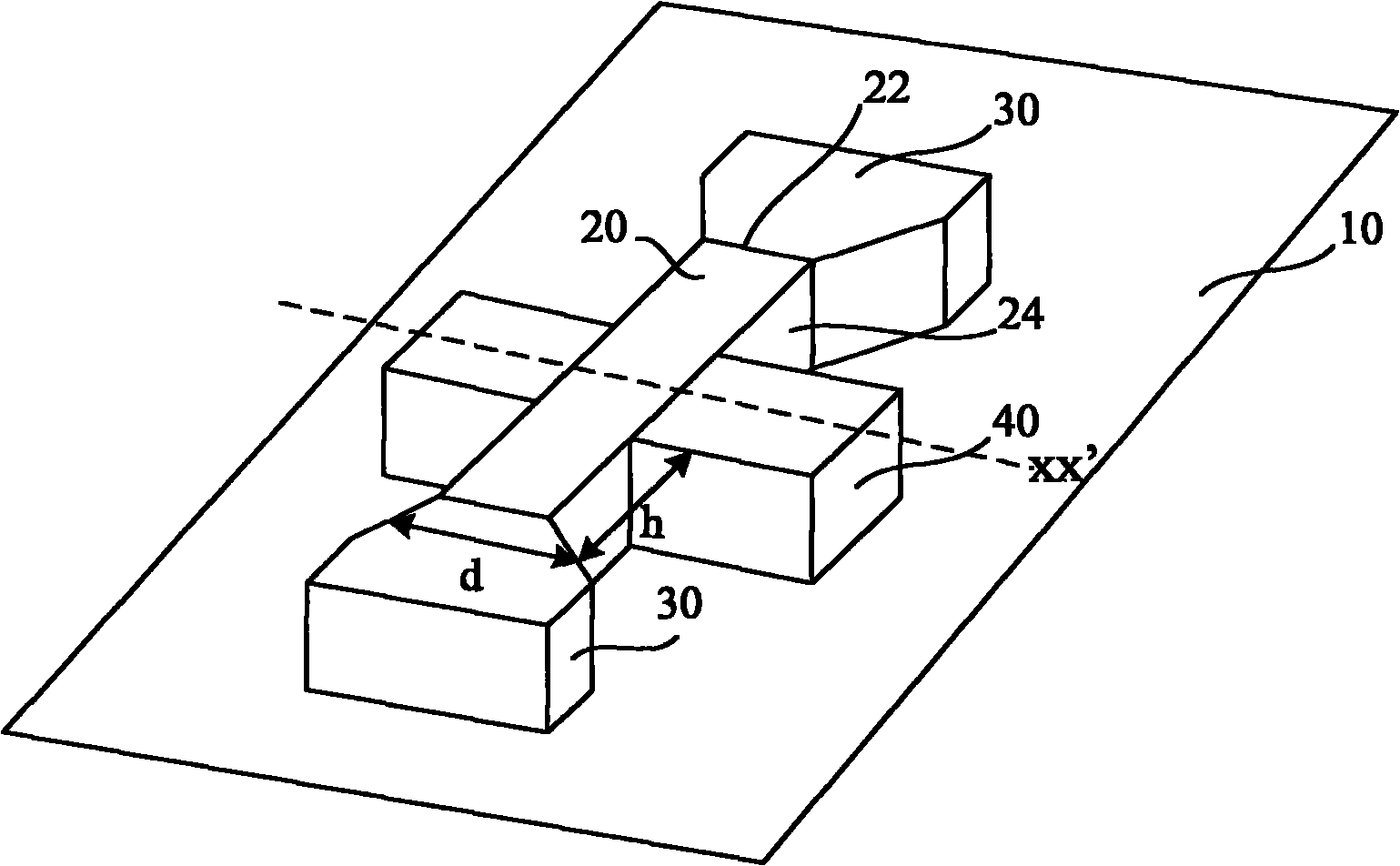
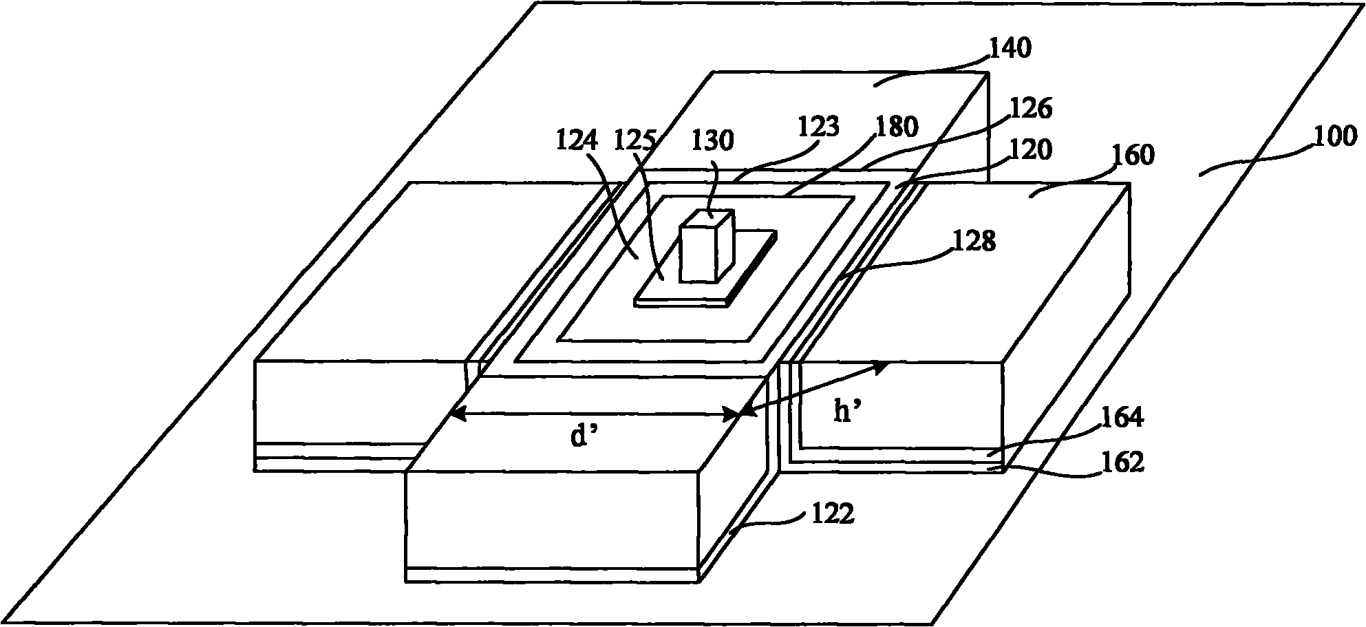
[0083] The disclosure below provides many different embodiments or examples for realizing the technical solution provided by the present invention. Although components and arrangements of specific examples are described below, they are examples only and are not intended to limit the invention.

[0084] Furthermore, the present invention may repeat reference numerals and / or letters in different embodiments. This repetition is for simplicity and clarity and does not in itself indicate a relationship between the various embodiments and / or arrangements discussed.

[0085] The present invention provides examples of various specific processes and / or materials, however, alternative applications of other processes and / or other materials that can be realized by those skilled in the art obviously do not depart from the scope of the present invention. It should be emphasized that in this document, the relationship between various structures includes the necessary extension due to the ne...


PUM

PropertyMeasurementUnit
Thicknessaaaaaaaaaa

Abstract

The invention relates to a semiconductor device, which comprises a semiconductor substrate and a second gate, wherein the semiconductor substrate is positioned on an insulating layer; and the second gate is positioned on the insulating layer and partially embedded in the semiconductor substrate. A forming method for the semiconductor device comprises the following steps of: forming the semiconductor substrate on the insulating layer; forming a cavity in the semiconductor substrate, wherein the cavity is exposed out of the insulating layer; and forming the second gate, wherein at least part of the second gate is filled in the cavity. By the semiconductor device and the forming method thereof, a short channel effect, the resistance of a source region and a drain region and parasitic capacitance can be reduced.

Description

technical field [0001] The present invention relates to the technical field of semiconductors, in particular to a semiconductor device and a forming method thereof. Background technique [0002] As the channel length of MOSFET (Metal Oxide Field Effect Transistor) continues to shorten, a series of effects that can be ignored in the MOSFET long channel model become more and more significant, and even become the dominant factor affecting performance. This phenomenon is collectively referred to as short channeling effect. The short channel effect is easy to deteriorate the electrical performance of the device, such as causing a decrease in the gate threshold voltage, an increase in power consumption, and a decrease in the signal-to-noise ratio. [0003] In order to control the short channel effect, people have to dope more impurity elements such as phosphorus and boron into the channel, but this will easily lead to the decrease of carrier mobility in the channel of the device;...

Claims


Application Information

Patent Timeline
IPC IPC(8): H01L29/78H01L29/423H01L21/336H01L21/28
CPCH01L29/66795H01L29/785H01L29/66803
Inventor 朱慧珑梁擎擎
Owner INST OF MICROELECTRONICS CHINESE ACAD OF SCI
Why Eureka
Try Eureka