Multilayer body, method for producing same, electronic device member, and electronic device

A manufacturing method and technology of electronic equipment, which are applied in the fields of electrical components, electrical solid devices, chemical instruments and methods, etc., can solve the problem that the gas barrier properties of conductive electrode substrates cannot be said to be satisfactory enough, thin-film, lightweight, flexible The problems of chemical inversion, complicated manufacturing process, etc., to achieve the effects of excellent interlayer adhesion, excellent gas barrier properties, and high-efficiency manufacturing

Active Publication Date: 2012-01-11
LINTEC CORP
View PDF9 Cites 5 Cited by
  • Summary
  • Abstract
  • Description
  • Claims
  • Application Information

AI Technical Summary

Problems solved by technology

[0005] However, the gas barrier properties of the conductive electrode substrates described in these documents cannot be said to be sufficiently satisfactory, and further improvement is required.
In addition, since the adhesion between the surface smoothing layer and the inorganic barrier layer and between these layers and the electrode (conductive electrode layer) is insufficient, it is sometimes necessary to provide a functional film for improving the adhesion between the layers, and the manufacturing process is cumbersome. And there are problems that are contrary to thin film, light weight and flexibility

Method used


Image

  • Multilayer body, method for producing same, electronic device member, and electronic device
  • Multilayer body, method for producing same, electronic device member, and electronic device
  • Multilayer body, method for producing same, electronic device member, and electronic device

Examples


Embodiment 1

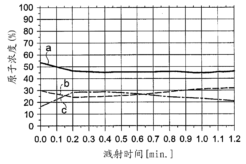
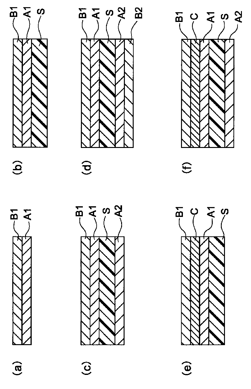
[0186]On a polyethylene terephthalate film ("PET38T-300", manufactured by Toray Co., Ltd., thickness: 38 μm) (hereinafter referred to as "PET film") as a base material, use a Meyer bar (Meyer bar) to coat Cloth silicone resin (A) (silicon release agent "KS835", manufactured by Shin-Etsu Chemical Co., Ltd.) mainly composed of polydimethylsiloxane as a polyorganosiloxane compound, and heat at 120°C for 2 minutes to form A layer containing the silicon release agent A with a thickness of 100 nm was obtained to obtain a molded product. Next, use the figure 2 The plasma ion implantation apparatus shown implanted nitrogen into the surface of the layer containing polydimethylsiloxane by plasma ion implantation to produce a molded body 1 .

[0187] The conditions of plasma ion implantation are as follows.

[0188] ? Plasma generating gas: N 2

[0189] ? Duty cycle: 0.5%

[0190] ? Repeat frequency: 1000Hz

[0191] ? Applied voltage: -10kV

[0192] ? RF power supply: frequency 1...

Embodiment 2

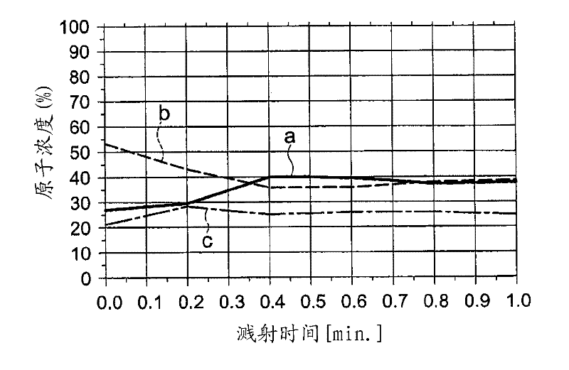
[0206] The molded body 2 was fabricated in the same manner as in Example 1 except that argon (Ar) was used as the plasma generation gas.

[0207] Next, in the same manner as in Example 1, on the ion-implanted polyorganosiloxane compound layer of the molded body 2, an ITO film having a thickness of 50 nm as a conductor layer was formed by magnetron sputtering to produce a film having a thickness of 50 nm. A laminate 2 composed of a substrate layer (PET film)-A layer (polyorganosiloxane-based compound layer ion-implanted with argon)-B layer (ITO film).

Embodiment 3

[0209] The compact 3 was produced in the same manner as in Example 1 except that helium (He) was used as the plasma generation gas.

[0210] Next, in the same manner as in Example 1, on the ion-implanted polyorganosiloxane compound layer of the compact 3, an ITO film having a thickness of 50 nm as a conductor layer was formed by magnetron sputtering to produce a film having a thickness of 50 nm. A laminate 3 composed of a substrate layer (PET film)-A layer (polyorganosiloxane compound layer ion-implanted with helium)-B layer (ITO film).


PUM

PropertyMeasurementUnit
thicknessaaaaaaaaaa
depthaaaaaaaaaa
depthaaaaaaaaaa

Abstract

Disclosed is a multilayer body which comprises at least a conductor layer and a gas barrier layer that is configured from a material containing oxygen atoms, carbon atoms and silicon atoms. The multilayer body is characterized in that the present ratio of oxygen atoms in the gas barrier layer gradually decreases from the surface of the gas barrier layer to the depth direction, while the present ratio of carbon atoms gradually increases. Also disclosed are a method for producing the multilayer body, an electronic device member which is composed of the multilayer body, and an electronic device which comprises the electronic device member. The multilayer body exhibits excellent gas barrier properties and excellent interlayer adhesion, while comprising a conductor layer with high surface smoothness. Since the multilayer body can be flexible and light-weighted, the multilayer body is suitable for use as an electronic device member for an organic EL display, a solar cell and the like. In addition, since the multilayer body can be produced by a roll-to-roll mass production process, the multilayer body can be produced at low cost.

Description

technical field [0001] The present invention relates to a laminate having a gas barrier layer and a conductor layer having excellent gas barrier properties and excellent interlayer adhesion, and a method for producing the laminate, an electronic device member including the laminate, and an electronic device having the same Electronic equipment with components. Background technique [0002] In recent years, in displays such as liquid crystal displays and electroluminescent (EL) displays, research has been conducted on using transparent plastic films instead of glass plates as substrates with electrodes in order to achieve thinner, lighter, and more flexible displays. [0003] However, since plastic films are more permeable to water vapor, oxygen, etc. than glass plates, there are problems of easy deterioration of internal components of the display and low surface smoothness. [0004] In order to solve this problem, Patent Documents 1 and 2 propose conductive electrode substr...

Claims


Application Information

Patent Timeline
Patent Type & Authority Applications(China)
IPC IPC(8): B32B27/00B32B7/02G02F1/1333G09F9/30
CPCH01L51/5256G02F2201/50C08J7/123C08J7/04C08J2383/04G02F1/133305Y10T428/31663B32B27/06B32B7/02G02F1/1333G09F9/30H10K50/8445
Inventor 星慎一近藤健
Owner LINTEC CORP
Why Eureka
Try Eureka