Circular-arc microstrip curve plane slow wave device

A circular arc and microstrip technology, applied in the field of semicircular arc microstrip curved plane slow wave devices, can solve the problems of low coupling impedance and output power, difficulty in meeting strength requirements, poor heat dissipation, etc., and achieve improved coupling impedance and Effects of output power, improvement of strength and heat dissipation, and avoidance of reflection phenomenon

Inactive Publication Date: 2013-12-11
UNIV OF ELECTRONICS SCI & TECH OF CHINA
View PDF3 Cites 0 Cited by
  • Summary
  • Abstract
  • Description
  • Claims
  • Application Information

AI Technical Summary

Problems solved by technology

[0008] Although this type of microstrip curved planar slow-wave device is used in conjunction with a microwave traveling-wave tube, it has a good effect, but when it is used in conjunction with a traveling-wave tube working above the millimeter-wave frequency band, the structural size of the slow-wave device will become smaller. It is very small and requires high processing precision for the corner of the right angle, and it is often difficult to realize the actual processing accurately; and the mismatch caused by the sudden change at the right angle will cause the reflection of the wave, and when the size of the microstrip curve is very small, at the tip of the right angle It is also easy to produce tip discharge effect; in addition, the substrate is made of alumina ceramics with a purity of 99%, and the relative permittivity of alumina ceramics is relatively high (ε r =9.6), the thickness of the substrate is 1.35mm when working in the S-band, and the alumina ceramic substrate can still be used; but when the traveling wave tube works in the W-band (94-97GHz), the substrate is required to be very thin (the thickness is more than ten micron), the alumina ceramics at this time are easily broken, and the thermal conductivity of alumina ceramics (W·(m·K) -1 ) is only 25.5, and its heat dissipation performance is still relatively poor, which not only affects the yield of the device, but also affects the further improvement of the performance of this type of planar slow wave device. The coupling impedance of the square waveform microstrip curve planar slow wave device and relatively low output power
The above-mentioned "square wave" microstrip curve is due to the wave reflection caused by the abrupt change of the microstrip curve at the right-angled corner, and the discharge effect is easily generated at the corner tip of the right angle. In addition, the use of alumina ceramics as the substrate not only has poor heat dissipation, but also Its performance is difficult to meet the strength requirements when working in the frequency band above the millimeter wave because of its fragility
Therefore, the above-mentioned background technology has defects such as difficulty in miniaturizing the structure of the device, poor heat dissipation of the substrate, supporting the use of traveling wave tubes operating in the frequency range above millimeter waves, poor performance and reliability, relatively low coupling impedance and output power, etc.

Method used


Image

  • Circular-arc microstrip curve plane slow wave device
  • Circular-arc microstrip curve plane slow wave device
  • Circular-arc microstrip curve plane slow wave device

Examples


Embodiment Construction

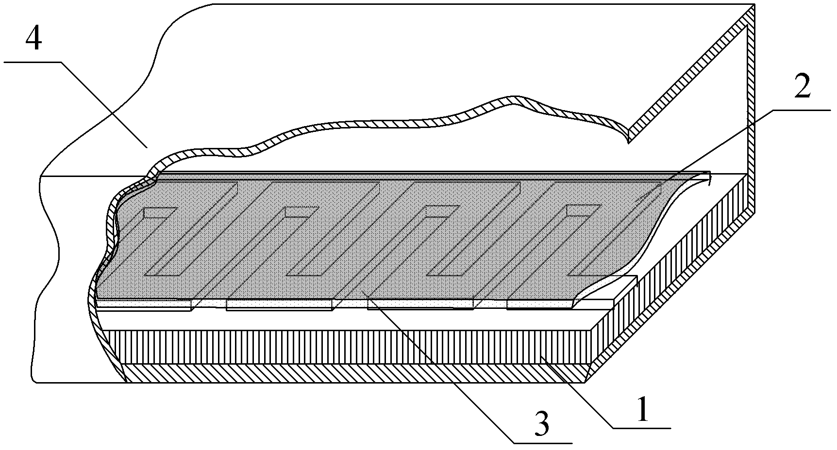
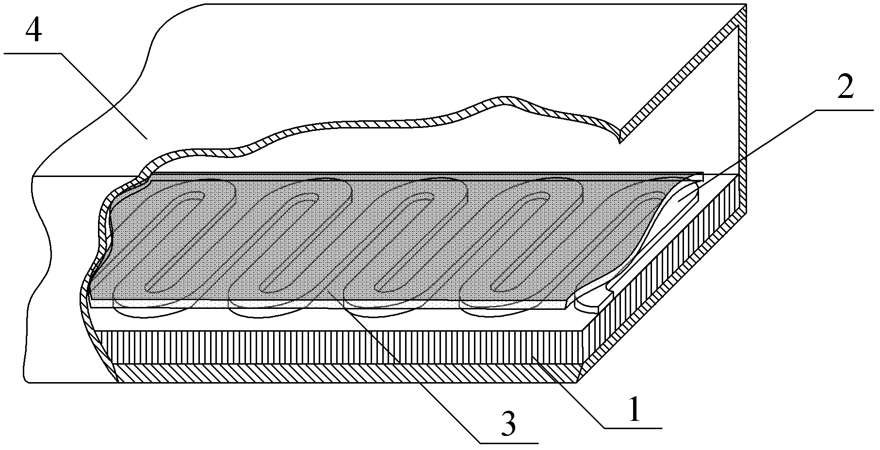
[0017] In this embodiment, an arc-shaped microstrip curved planar slow-wave device working in the 90-110 GHz band is taken as an example, in which: the substrate 1 (length×width×thickness) is 14.72×0.5×0.05mm, and the material is Purity 99wt%, relative permittivity ε r =4, boron nitride with loss tangent tanδ=0.00025; the line body (length×width×thickness) of the microstrip line 2 is 81.48×0.04×0.015mm, the material is metal Cu, and the microstrip curve has a total of 92 periods. The microstrip curve is 14.72mm long along the electron beam direction (that is, each cycle is 0.16mm long along the electron beam direction), the interval between two adjacent parallel microstrips is 0.04mm, and the inner radius of the semicircular microstrip curve at the connection part Both are R0.02mm; the metal shell 4 (length×width×height) is 14.72×0.6×0.4mm; when used together, the front and rear ends are respectively connected to the electron gun and collector of the traveling wave tube. In t...


PUM


Abstract

The invention belongs to a circular-arc microstrip curve plane slow wave device which is assorted with a travelling wave tube in a microwave vacuum electronic technology. The circular-arc microstrip curve plane slow wave device comprises a boron nitride substrate, a semicircular microstrip curve and a metal shell, wherein the semicircular microstrip curve is fixed on the substrate and has an input end and an output end. According to the invention, because the microstrip curve the connection part of which is a smooth semicircular-arc is adopted, and boron nitride which has low dielectric constant and higher compression strength, hardness and heat conductivity factor is used as the substrate, not only the coupling impedance and the output power are improved, but also the strength and the heat dissipation of the substrate as well as the finished product ratio and the service life in the production process of the slow wave device are effectively improved. Therefore, the microstrip curve plane slow wave device can work in a frequency band above millimeter waves stably and reliability at the same time of being miniaturized and has the characteristics of good heat dissipation and high coupling impedance and output power, high performance and reliability while cooperatively used with the travelling tube working in a frequency band above millimeter waves, as well as high finished product rate and long service life in the production process of the slow wave device, and the like.

Description

technical field [0001] The invention belongs to the field of microwave vacuum electronics technology and is matched with a slow-wave device for traveling wave tubes, in particular to a semi-circular arc-shaped microstrip curve plane slow-wave device. Background technique [0002] Traveling wave tube is a vacuum electronic device that realizes microwave amplification by continuously modulating the speed of electron beam. In the traveling wave tube, the electron beam interacts effectively with the electromagnetic traveling wave traveling in the slow wave device. In the slow wave circuit with dozens of wavelengths, the electron beam continuously transfers the kinetic energy of the electrons to the electromagnetic traveling wave. , so that the electromagnetic traveling wave is amplified. Traveling wave tubes have the characteristics of high power, high efficiency, high gain, wide frequency band and long life. [0003] The slow wave device is the main component for amplifying m...

Claims


Application Information

Patent Timeline
Patent Type & Authority Patents(China)
IPC IPC(8): H01J23/24
Inventor 段兆云刁鹏林娴静
Owner UNIV OF ELECTRONICS SCI & TECH OF CHINA
Why Eureka
Try Eureka