Substrate, epitaxial wafer and semiconductor device
A substrate and body technology, applied in the fields of substrates, epitaxial wafers and semiconductor devices, can solve problems such as poor flatness, and achieve the effects of reducing subsequent production costs, improving flatness, and improving product quality
- Summary
- Abstract
- Description
- Claims
- Application Information
AI Technical Summary
Problems solved by technology
Method used
Image

Examples
Embodiment 1-4
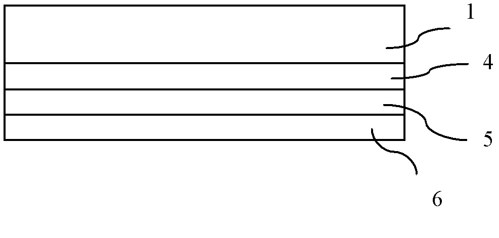
[0041] figure 2 It is a schematic diagram of the substrate structure for epitaxial wafers in Examples 1-4. Such as figure 2 As shown, the substrate includes a substrate body 1, and the substrate body 1 can be N-type, that is, doped with arsenic, phosphorus or antimony; the substrate body 1 can also be P-type, that is, doped with boron element. A first silicon dioxide layer 4 is arranged on the rear side of the substrate body 1 . A polysilicon layer 5 is provided on the surface of the first silicon dioxide layer 4 . The surface of the polysilicon layer 5 is provided with a second silicon dioxide layer 6
[0042] Deposition of silicon dioxide and polysilicon can be achieved by existing technologies.
[0043] Embodiments 1-4 are heavy arsenic-doped substrate bodies, the difference between the two is that in embodiments 1-4, the back of the substrate body is provided with first dioxide Silicon layer: polysilicon layers with thicknesses of 6um, 7.7um, 8.8um, and 9.7um, and ...
Embodiment 5-8
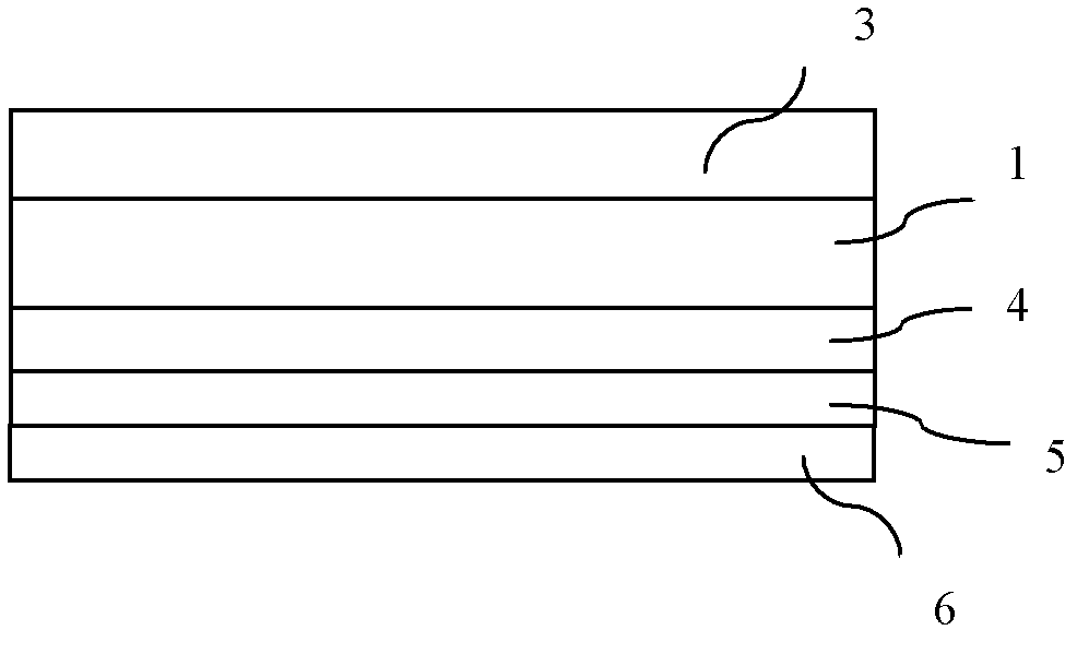
[0045] image 3 It is a schematic diagram of the epitaxial wafer structure in Embodiment 5-8. Such as image 3 As shown, Examples 5-8 use the substrates in Examples 1-4 to grow epitaxial layers respectively. Fabricated epitaxial wafer structures such as image 3 shown, epitaxial wafers, including figure 2 In the shown substrate, an epitaxial layer 3 is grown on the front surface of the substrate body 1 . The substrate includes a substrate body 1 , and a first silicon dioxide layer 4 is provided on the back of the substrate body 1 . The surface of the first silicon dioxide layer 4 is provided with a polysilicon layer 5 . The surface of the polysilicon layer 5 is provided with a second silicon dioxide layer 6 . The epitaxial layer 3 is arranged on the front surface of the substrate body 1 .
[0046] In Comparative Examples 1-4, the first silicon dioxide layer, the polysilicon layer and the second polysilicon layer are not arranged on the backside of the heavy arsenic-dop...
Embodiment 9-12
[0068] Figure 4 It is a schematic diagram of the substrate structure in Examples 9-12. Such as Figure 4 As shown, the substrate includes a substrate body 1 , and a first silicon dioxide layer 4 is provided on the back of the substrate body 1 . The surface of the first silicon dioxide layer 4 is provided with a polysilicon layer 5 . The surface of the polysilicon layer 5 is provided with a second silicon dioxide layer 6 . The substrate body 1 has a monocrystalline silicon layer 2 on the front side. The thickness of the single crystal silicon layer 2 is 2-5 μm. Its specific thickness can be determined according to the overall thickness of the epitaxial wafer and the thickness of the substrate body. The higher the substrate thickness, the thicker the monocrystalline silicon layer. In subsequent production, an epitaxial layer is grown on the surface of the single crystal silicon layer 2 .
[0069] The substrate body 1 can be N-type, that is, doped with arsenic, phosphorus...
PUM
| Property | Measurement | Unit |
|---|---|---|
| Thickness | aaaaa | aaaaa |
| Thickness | aaaaa | aaaaa |
| Thickness | aaaaa | aaaaa |
Abstract
Description
Claims
Application Information