High-power semiconductor chip laser array

A thin-film laser and semiconductor technology, used in semiconductor lasers, semiconductor laser excitation devices, lasers, etc., can solve the problems of single laser wavelength range, large laser volume, and low service life, and achieve favorable heat dissipation, high beam quality, and stability. Good results

Inactive Publication Date: 2012-01-18
CHONGQING NORMAL UNIVERSITY
View PDF1 Cites 0 Cited by
  • Summary
  • Abstract
  • Description
  • Claims
  • Application Information

AI Technical Summary

Problems solved by technology

[0003] In the prior art, in order to increase the power of solid-state lasers, a solid-state thin-sheet laser using a diode laser array as a pumping source has appeared, and the output laser power after pumping is relatively high; although theoretically it is possible to increase the output power of the laser, the gain medium It is a common gain medium for general solid-state lasers, and the laser wavelength range is relatively single; the resonant cavity is composed of a reflector, a gain medium, and a transmission mirror, and the resonant cavity and beam shaping are independent, resulting in a laser with large volume, difficult heat dissipation, and large optical loss. Disadvantages, so the service life is lower and the efficiency is poorer

Method used


Image

  • High-power semiconductor chip laser array
  • High-power semiconductor chip laser array

Examples


Embodiment Construction

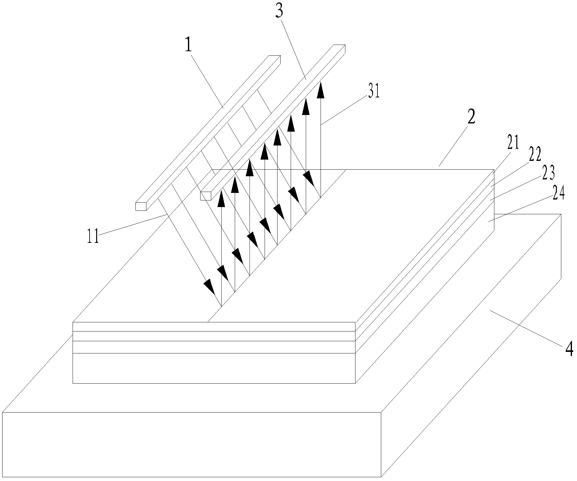
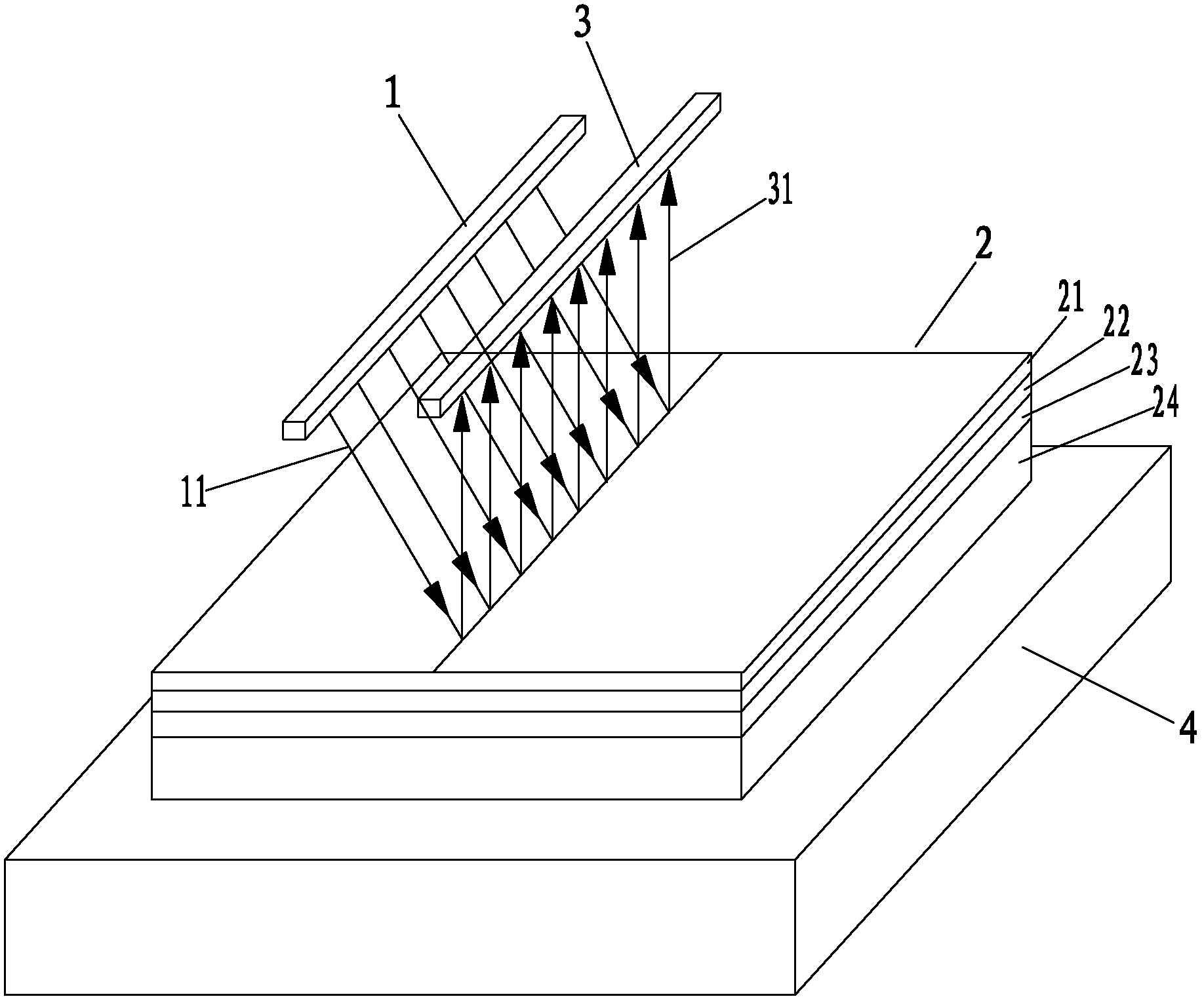
[0015] figure 1 It is a schematic diagram of the structural principle of the present invention, as shown in the figure: the high-power semiconductor thin-disk laser array of this embodiment includes a pump light source system 1, a semiconductor gain thin slice 2 and a microcavity mirror array 3, a semiconductor gain thin slice 2 and a microcavity The mirror array 3 forms a resonant cavity, and the pump light source system 1 includes a semiconductor laser array and a shaping component. The semiconductor laser array is shaped by the shaping component to form a pumping beam array 11, and the pumping beam array 11 is incident on the semiconductor gain The sheet 2, the microcavity mirror array 3 is used to output the laser array 31.

[0016] In this embodiment, the semiconductor gain sheet 2 includes a heat dissipation window layer 21, a multi-quantum well active layer 22 and a distributed Bragg reflection layer 23 from top to bottom; The stacking method of capillary bonding techn...


PUM


Abstract

The invention discloses a high-power semiconductor chip laser array. The high-power semiconductor chip laser array comprises a pump light source system, a semiconductor gain chip and a microcavity lens array, wherein the semiconductor laser array forms a pump beam array after the semiconductor laser array is shaped by a shaping component; the pump beam array enters the semiconductor gain chip; and the microcavity lens array is used for forming a resonant cavity array and for being coupled with an output laser array. According to the invention, the gain medium is a semiconductor chip which can be self-designed according to the species of semiconductor materials, the ingredients of the materials, and the difference of the thicknesses of quantum wells, and the wavelengths of lasers are from visible lights to near-infrared lights, thus the defect that the wavelength of lasers emitted by the gain medium is relatively fixed in the prior art is overcome; the laser array has an unique advantage in application to aspects, such as optical integration, optical communications, optical interconnections and high-speed parallel computations; heat is dispersed to a plurality of units, thus the high-power semiconductor chip laser array is more beneficial to heat dispersion of a laser and can output higher total power; in addition, the high-power semiconductor chip laser array has the advantages of small volume as a whole, good stability, strong reliability and high efficiency.

Description

technical field [0001] The invention relates to the field of laser technology, in particular to a high-power semiconductor thin-chip laser array. Background technique [0002] Diode-pumped solid-state laser technology has broad application prospects in various fields, and high-power diode-pumped solid-state lasers also have good development prospects. How to obtain high-power laser output, wide wavelength range, high output efficiency and long service life are the problems that high-power lasers need to solve. [0003] In the prior art, in order to increase the power of solid-state lasers, a solid-state thin-sheet laser using a diode laser array as a pumping source has appeared, and the output laser power after pumping is relatively high; although theoretically it is possible to increase the output power of the laser, the gain medium It is a common gain medium for general solid-state lasers, and the laser wavelength range is relatively single; the resonant cavity is compose...

Claims


Application Information

Patent Timeline
Patent Type & Authority Applications(China)
IPC IPC(8): H01S5/04H01S5/34H01S5/125
Inventor 戴特力张鹏梁一平范嗣强
Owner CHONGQING NORMAL UNIVERSITY
Why Eureka
Try Eureka