Method for controlling critical size of graph on uneven silicon slice surface

A critical dimension, silicon wafer surface technology, applied in semiconductor/solid-state device manufacturing, photolithography process exposure devices, electrical components, etc. Large and other problems, to achieve the effect of improving the excellent rate

Active Publication Date: 2012-02-01
SEMICONDUCTOR MANUFACTURING INTERNATIONAL (BEIJING) CORP +1
View PDF5 Cites 13 Cited by
  • Summary
  • Abstract
  • Description
  • Claims
  • Application Information

AI Technical Summary

Problems solved by technology

[0016] (2) In the same batch of silicon wafers, the critical dimension CD of the pattern of the tunneling injection mask layer of different silicon wafers may be different, such as image 3 as shown ( image 3 The exposure energy of each silicon wafer in is the same, the ordinate indicates the size of the critical dimension CD of the tunneling injection mask layer, and the abscissa is used to mark the silicon wafer, for example, #1 indicates the first silicon wafer in a batch, #2 Indicates the second silicon wafer in the same batch, ..., and so on), from image 3 It can be seen that for different silicon wafers of the same batch, the critical dimension of the tunneling implantation mask layer sometimes varies greatly. For example, the critical dimension of the tunneling implantation mask layer of the fifth silicon wafer is 0.61 μm, while The critical dimension of the tunneling implant mask layer of the tenth silicon wafer is 0.653 μm, which means that the critical dimension CD of the tunnel implant mask layer of some silicon wafers in a batch of silicon wafers does not meet the process requirements

Method used


Image

  • Method for controlling critical size of graph on uneven silicon slice surface
  • Method for controlling critical size of graph on uneven silicon slice surface
  • Method for controlling critical size of graph on uneven silicon slice surface

Examples


Embodiment Construction

[0036] The following will combine Figure 5 ˜ FIG. 8 further describes in detail the method for controlling the critical dimensions of the graphics on the surface of the uneven silicon wafer according to the present invention.

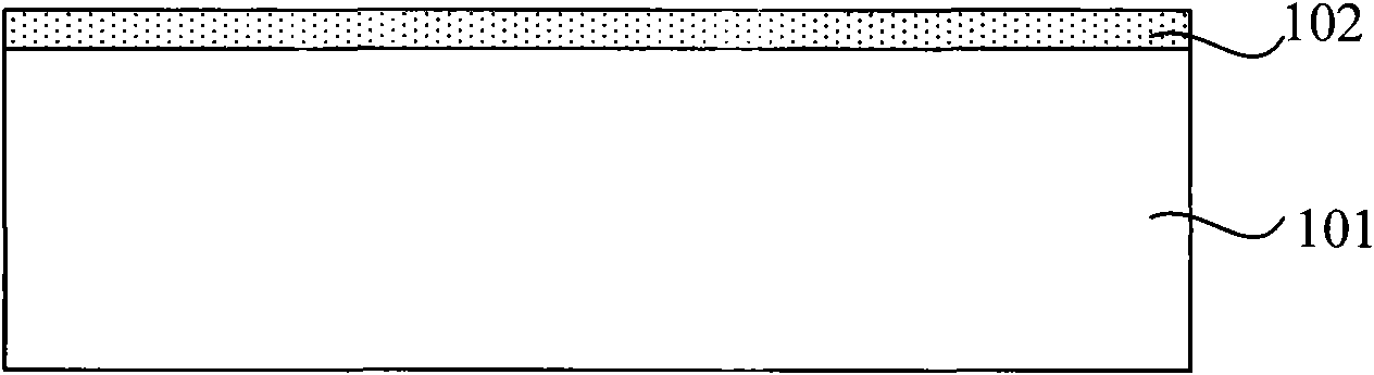
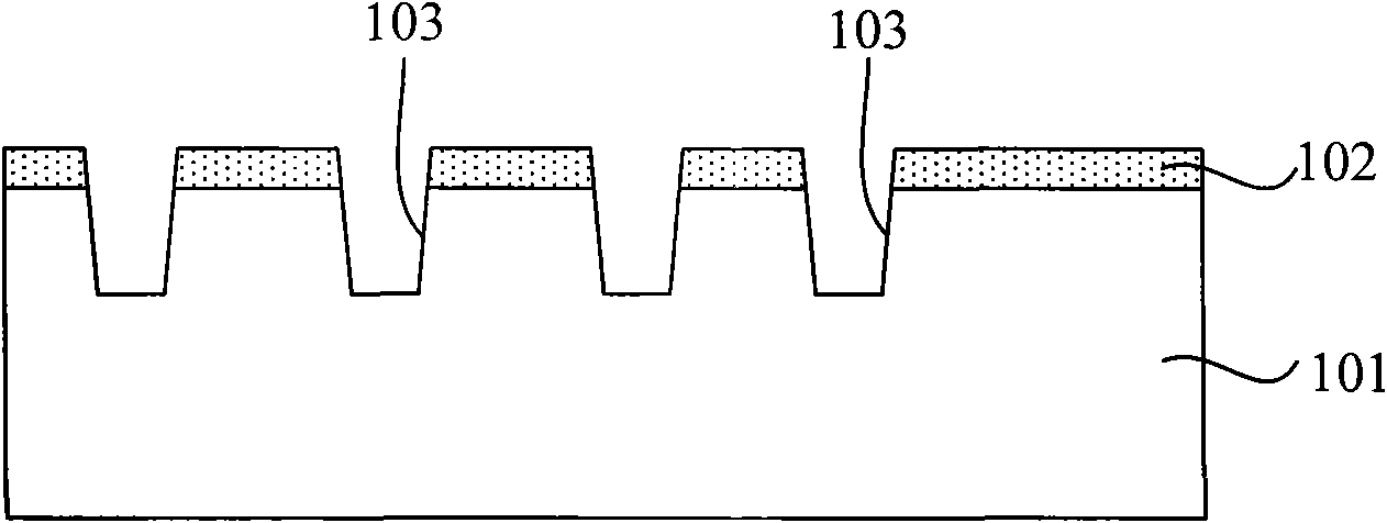
[0037] In order to characterize the unevenness of the surface of the silicon wafer, a physical concept-step height is introduced. The definition of the step height is the distance between the highest point and the lowest point on the surface of the silicon wafer. For example, as Figure 1D As shown, when fabricating the tunneling injection mask layer, the height difference H between the top of the isolation trench and the surface of the substrate is the step height.

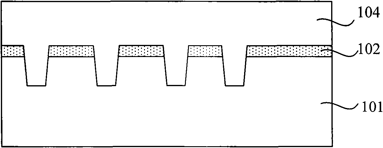
[0038]The manufacture of semiconductor devices is performed step by step according to preset process conditions, for example, when making a tunneling injection mask layer, the thickness of the deposited barrier layer, the depth of the etched trench, the thickness of the deposited oxide, t...


PUM


Abstract

The invention relates to a method for controlling a critical size of a graph on an uneven silicon slice surface, which comprises the following steps that: establishing a relation curve of a step height and the critical size, and the step height is a distance between a highest point and a lowest point on the surface of a silicon slice; measuring a real step height; judging whether the real step height is equal to a setup value, if the real step height is equal to the setup value, exposing photosensitive resist according to a setup exposure energy, and if the real step height is not equal to the setup value, executing a next step; utilizing a formula Esplit= Ebaseline + (CDsplit - CDBASELINE) * Slop to calculate the exposure energy, exposing the photosensitive resist according to the calculated exposure energy Esplit, wherein the Esplit indicates the real exposure energy, Ebaseline indicates the setup exposure energy, CDsplit is a critical size corresponding to the real step height in the relation curve of the step height and the critical size, CDbaseline is a critical size corresponding to the step height setup value in the relation curve of the step height and the critical size, and Slop is a constant.

Description

technical field [0001] The invention relates to semiconductor manufacturing technology, in particular to a method for controlling the critical dimension of graphics on the surface of an uneven silicon chip. Background technique [0002] The purpose of photolithography is to copy the pattern on the photomask to the surface of the silicon wafer. The CD (critical dimension) of the pattern copied to the surface of the silicon wafer must meet the process requirements, otherwise, the silicon wafer cannot enter the subsequent process flow. [0003] Taking the TIM (tunnel implant mask) layer as an example, briefly introduce the photolithography process: [0004] Such as Figure 1A As shown, a barrier layer 102 is formed on the substrate 101, and the barrier layer 102 is usually a silicon nitride layer; [0005] Such as Figure 1B As shown, a trench 103 is etched on the substrate 101; [0006] Such as Figure 1C As shown, a deposited oxide 104 fills the trench 103; [0007] Such...

Claims


Application Information

Patent Timeline
Patent Type & Authority Applications(China)
IPC IPC(8): H01L21/02H01L21/66G03F7/20
Inventor 夏婷婷杨晓松郁志芳易旭东
Owner SEMICONDUCTOR MANUFACTURING INTERNATIONAL (BEIJING) CORP
Why Eureka
Try Eureka