Preparation method for silicon surface anti-reflection nanometer array structure

A technology of nano-array and array structure, which is applied in the field of preparation of controlling the surface nano-structure morphology, can solve the problems of rough and porous structure surface, reduce the performance of black silicon, enhance the surface recombination effect, etc., and achieve good broadband anti-reflection characteristics, Effect of improving photoelectric conversion performance and high surface minority carrier lifetime

Active Publication Date: 2012-02-15
INST OF PHYSICS - CHINESE ACAD OF SCI
View PDF4 Cites 23 Cited by
  • Summary
  • Abstract
  • Description
  • Claims
  • Application Information

AI Technical Summary

Problems solved by technology

This method requires fast laser pulses, and the equipment is expensive. More importantly, this method is point-by-point scanning. It takes a lot of time to make a large-area silicon micro-nano structure. At the same time, the preparation consistency is not good, and the preparation efficiency and output are low. , the surface of the structure is rough and porous, which will limit its practical application
[0006] In addition, it is particularly worth noting that the black silicon microstructure prepared by chemical methods and lasers has a large surface damage and a very rough surface. Although the optical properties are not greatly affected, it seriously affects the electrical properties of the microstructure surface.
For example, if the surface of the material is seriously damaged, the surface defects formed will increase accordingly, the surface recombination effect of minority carriers will increase, and the lifetime of minority carriers will decrease accordingly, which will greatly reduce the performance of black silicon in solar cells. The main reason why it is not widely used in the field of solar cells

Method used


Image

  • Preparation method for silicon surface anti-reflection nanometer array structure
  • Preparation method for silicon surface anti-reflection nanometer array structure
  • Preparation method for silicon surface anti-reflection nanometer array structure

Examples


preparation example Construction

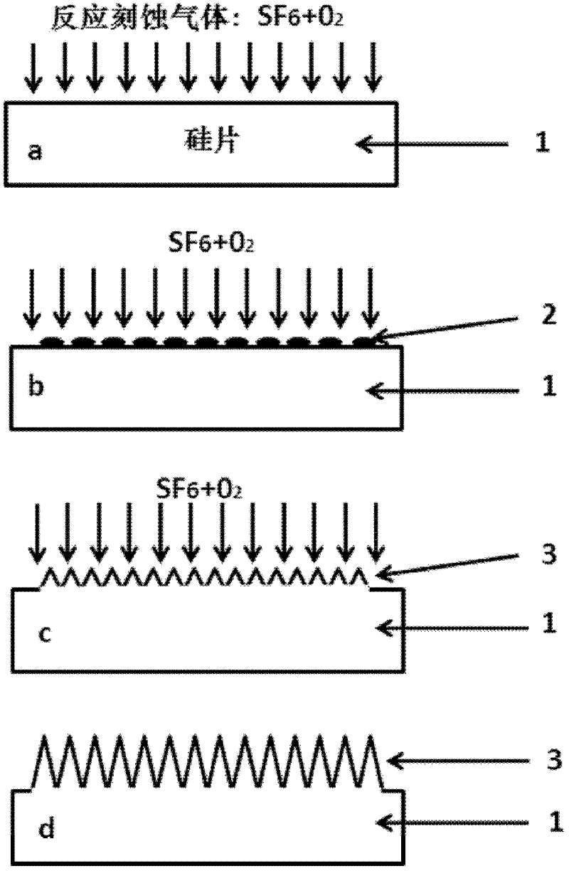
[0029] The preparation method of silicon surface super anti-reflection structure provided by the invention is as follows: figure 1 shown, including the following two steps:

[0030] 1) Wafer cleaning: put a 4-inch P(111) oriented monocrystalline silicon wafer 1 into acetone, alcohol and deionized water in order to ultrasonically clean it, and then dry it with nitrogen;

[0031] 2) Etching on the silicon wafer 1 to prepare the super anti-reflection structure on the silicon surface: put the silicon wafer 1 that has been ultrasonically cleaned in step 1 into the ICP system, and obtain the super anti-reflection structure 2 on the silicon surface through low-temperature etching. The specific process conditions As follows: the basic vacuum is about 1.0×10 -6 Torr, from -100°C to -140°C, SF 6 / O 2 The working pressure is 36 / 22-44 / 14, the working pressure is 6-25mTorr, the RIE power is 3-6W, the ICP power is 800-1000W, and the etching time is 7-17 minutes. Etching on the silicon w...

Embodiment 1

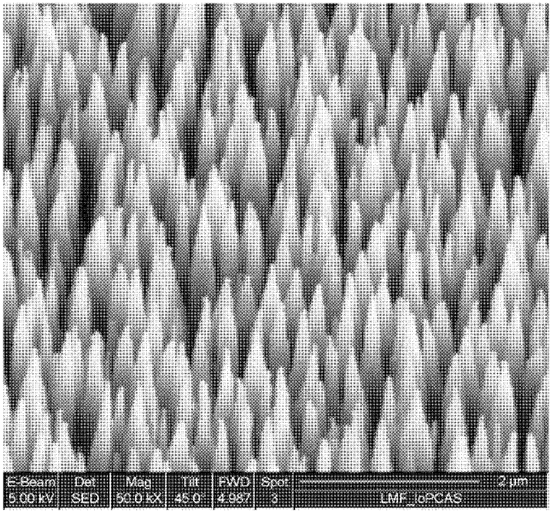
[0041] The surface morphology of the silicon surface super anti-reflection structure prepared in this embodiment can be found in Figure 6 a: The areal density of the super anti-reflective structure on the prepared silicon surface is about 1.3×10 9 / cm 2 , the height is about 1 μm, and the aspect ratio is between 10-20. Its detailed process flow is as follows:

[0042] 1) Clean the silicon wafer: take a 4-inch P(111) oriented monocrystalline silicon 1, use the traditional semiconductor cleaning process, clean it in acetone, alcohol and deionized water in sequence, and then dry it with nitrogen;

[0043] 2) Etching to obtain super anti-reflection surface nanostructures: put the single crystal silicon 1 cleaned in step 1) into the ICP system, and use a low-temperature etching process to prepare ultra-high anti-reflection structures 2 on the silicon surface. The specific process parameters are as follows: The base vacuum is about 1.0×10 -6 Torr, substrate temperature maintain...

Embodiment 2

[0045] The silicon surface super anti-reflection structure of this embodiment can be found in Figure 6 b: The areal density of the prepared silicon surface nanostructures is about 2.0×10 8 / cm 2 , the height is about 3.3 μm, and the aspect ratio is between 4-6. Its detailed process flow is as follows:

[0046] 1) Clean the silicon wafer: take a 4-inch P(111) oriented monocrystalline silicon 1, use the traditional semiconductor cleaning process, clean it in acetone, alcohol and deionized water in sequence, and then dry it with nitrogen;

[0047] 2) Etching to obtain nanostructures on the silicon surface: put the single crystal silicon 1 cleaned in step 1 into the ICP system, and use a low-temperature etching process to prepare black silicon 2. The specific process parameters are as follows: the basic vacuum is 1.0×10 -6 Torr, substrate temperature maintained at -120°C, SF 6 with O 2 The ratio is 40 / 18 (the unit is sccm), the working air pressure is maintained at 25mTorr, ...


PUM

PropertyMeasurementUnit
heightaaaaaaaaaa
heightaaaaaaaaaa
heightaaaaaaaaaa

Abstract

The invention relates to a preparation method for a silicon surface anti-reflection nanometer array structure, which comprises the following steps that: silicon chips are placed into an inductively coupled plasma (ICP) system, and nanometer conical array structures are obtained at the silicon surface under the conditions of the basic vacuum being 1.0*10<-6> Torr, the temperature being -100 DEG C to -140 DEG C, the gas flow rate ratio (SF6 / O2) being 36 / 22 to 44 / 14, the air pressure being 6 to 25mTorr, the reactive ion etching (RIE) power being 3 to 6W and the ICP power being 800 to 1000W. The method adopts a low-temperature etching technology, the masking process is not needed, the large-area silicon surface nanometer conical array structure with the super anti-reflection characteristic is directly prepared through etching, and in addition, the regulation and control on the nanometer conical structure feature is realized through regulating and controlling the corresponding parameters.

Description

technical field [0001] The present invention relates to a method for preparing super anti-reflection nanostructures on silicon surfaces, in particular to a method for preparing super anti-reflection nanostructures on silicon surfaces in a simple, rapid and large-scale manner and controlling the surface nanostructure morphology. Preparation. At the same time, the method for preparing the super anti-reflection nanostructure on the surface of silicon involved in the present invention does not have any requirements on the crystal orientation of silicon, so it is a silicon-based super anti-reflection structure that can be applied to single crystal silicon, polycrystalline silicon and amorphous silicon materials Preparation. More importantly, the method for preparing super anti-reflection nanostructures on silicon surfaces does not require a mask process, and the low-temperature etching preparation process greatly reduces the surface micro-damage to silicon materials, and prepares ...

Claims


Application Information

Patent Timeline
Patent Type & Authority Applications(China)
IPC IPC(8): C04B41/53
Inventor 孙旺宁李俊杰夏晓翔田士兵顾长志
Owner INST OF PHYSICS - CHINESE ACAD OF SCI
Why Eureka
Try Eureka