Welding disc and silicon-on-insulator (SOI) device with same

A technology of silicon-on-insulator and pads, which is applied to electric solid-state devices, semiconductor devices, semiconductor/solid-state device parts, etc., can solve the problem that it is not easy to form shallow trench isolation layers, the shallow trench isolation layer has limited height, and the spacing is enlarged. And other issues

Active Publication Date: 2012-02-29
SHANGHAI HUAHONG GRACE SEMICON MFG CORP
View PDF4 Cites 6 Cited by
  • Summary
  • Abstract
  • Description
  • Claims
  • Application Information

AI Technical Summary

Problems solved by technology

[0006] Through research, it is found that the above-mentioned pad structure that can reduce parasitic capacitance has obvious disadvantages: the formation of shallow trench isolation layer needs chemical mechanical planarization (CMP) process to complete, because CMP has a castellation (Disshing) effect, it is generally not easy Realize the formation of a shallow trench isolation layer in the area directly below the pad metal layer; in addition, the characteristics of the preparation process of the shallow trench isolation layer determine that the height of the shallow trench isolation layer (depth in the Z direction) is limited, which will limit the upper and lower poles. The expansion of the spacing between the boards further limits the effect of reducing the parasitic capacitance

Method used


Image

  • Welding disc and silicon-on-insulator (SOI) device with same
  • Welding disc and silicon-on-insulator (SOI) device with same
  • Welding disc and silicon-on-insulator (SOI) device with same

Examples


Embodiment 1

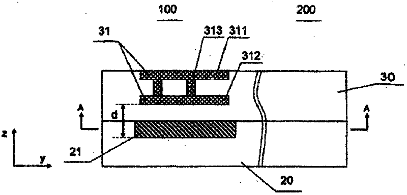
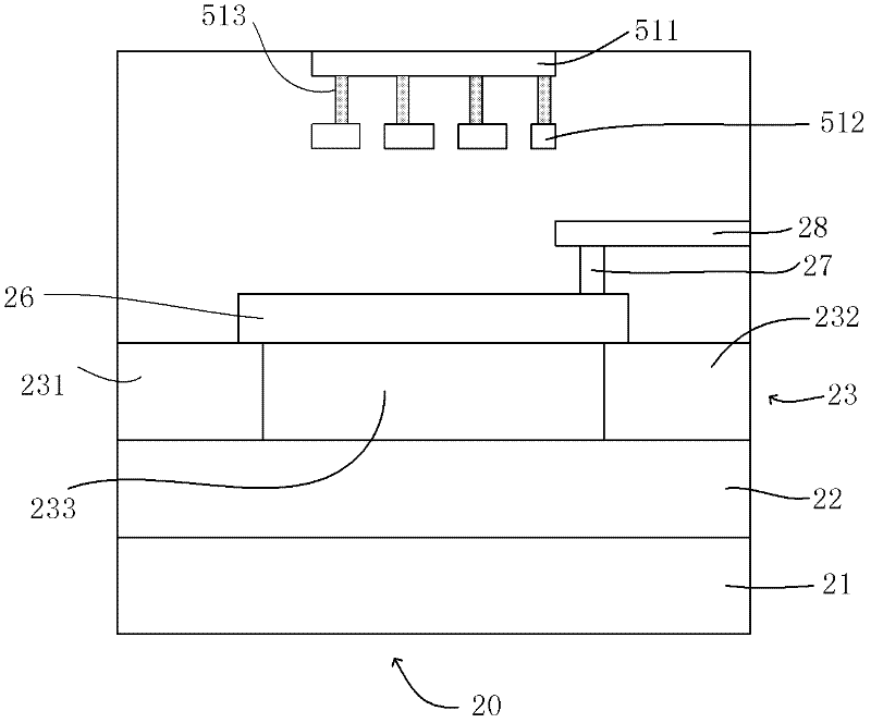
[0044] Such as image 3 As shown, the silicon-on-insulator device includes a silicon-on-insulator substrate 20, and the silicon-on-insulator substrate 20 includes a silicon substrate 21, a buried oxide layer 22 formed on the silicon substrate, and a silicon layer 23 formed on the buried oxide layer, The silicon layer 23 can be used to form various semiconductor devices. Wherein, a source region 231 , a drain region 232 of the transistor and an STI isolation region 233 for isolating the source region and the drain region are formed on the silicon layer 23 . The source region 231 and the drain region 232 are source regions or drain regions of two different transistors in a silicon-on-insulator device.

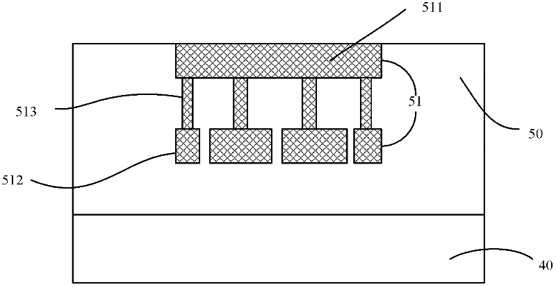
[0045] The silicon-on-insulator device further includes the above-mentioned pad, which includes several pad metal layers, the pad metal layer 512 close to the semiconductor substrate is divided into several parts separated from each other, the pad metal layer 512 close to the se...

Embodiment 2

[0052] Such as Figure 4 As shown, the silicon-on-insulator device includes a silicon-on-insulator substrate 20, and the silicon-on-insulator substrate 20 includes a silicon substrate 21, a buried oxide layer 22 formed on the silicon substrate, and a silicon layer 23 formed on the buried oxide layer, Silicon layer 23 can be used to form various devices. Specifically, a source region 231 , a drain region 232 and an STI isolation region 233 for isolating the source region and the drain region are formed on the silicon layer. The source region 231 and the drain region 232 are the source regions or drain regions of two different transistors in the silicon-on-insulator device, and the STI isolation region 233 is formed using a conventional shallow trench isolation process, including a trench formed in the silicon-on-insulator substrate. trench, trench fill oxide, which may be silicon oxide. The bottom of the STI isolation region 233 extends to the interface between the silicon su...


PUM


Abstract

The invention discloses a welding disc, which comprises a plurality of welding disc metal layers, wherein the welding disc metal layers close to a semiconductor gasket and a semiconductor substrate form a parasitic capacitor; and the welding disc metal layers close to the semiconductor substrate are partitioned into parts which are separated from one another to reduce the opposite area of two pole plates of the parasitic capacitor, so that a parasitic capacitance value is reduced. The invention also discloses a silicon-on-insulator (SOI) device. The device comprises the welding disc, wherein a conductive layer which is used as a shielding layer is arranged inside the welding disc, so that a non-linear changeable parasitic capacitor inside an integrated circuit is changed into a constant parasitic capacitor; further, a shallow trench isolation (STI) area with increased depth is arranged inside the SOI device, so that the parasitic capacitance value is reduced. When the SOI device is operated, a radio frequency signal applied onto the device can be leaked out of the parasitic capacitor as few as possible; and the acquired radio frequency signal is a linear signal and meets the using requirement of radio frequency equipment.

Description

technical field [0001] The invention relates to a pad of a semiconductor integrated circuit, in particular to a pad in a radio frequency manufacturing process; the invention also relates to a silicon-on-insulator device with the pad. Background technique [0002] In the field of semiconductor manufacturing, after the integrated circuit is manufactured, a pad is usually formed above the interconnection structure layer, and the pad is electrically connected to the internal circuit as an interface between the internal circuit and the external signal circuit. [0003] At the same time, as the feature size of the chip continues to decrease, the speed of the chip is required to be faster and faster, and the requirements for the parasitic capacitance formed inside various semiconductor devices are getting higher and higher. The smaller the parasitic capacitance, the better the running speed and frequency characteristics of the chip, and the less signal leakage from the parasitic ca...

Claims


Application Information

Patent Timeline
Patent Type & Authority Applications(China)
IPC IPC(8): H01L23/522H01L27/12
Inventor 李乐
Owner SHANGHAI HUAHONG GRACE SEMICON MFG CORP
Why Eureka
Try Eureka