
Electrostatic discharge (ESD) protection structure between silicon-on-insulator (SOI)/CMOS integrated circuit power supply and ground

An ESD protection, integrated circuit technology, applied in circuits, electrical components, electrical solid devices, etc., can solve the problems of ESD damage, functional failure, surge, etc., to achieve the effect of easy implementation, simple structure, and compatible process steps

Inactive Publication Date: 2012-02-29
58TH RES INST OF CETC
View PDF5 Cites 2 Cited by
  • Summary
  • Abstract
  • Description
  • Claims
  • Application Information

AI Technical Summary

Problems solved by technology

But in practical applications, the reverse breakdown voltage (V B ) is close to or even higher than the junction breakdown voltage of the SOI device, it often occurs that the SOI device inside the circuit has a junction breakdown under the stress condition of ESD, and the SOI diode has not started to work due to the high reverse breakdown voltage, which eventually causes the circuit According to the sudden increase of the quiescent current of the chip from the μA level to the tens of mA level, the interior is damaged by ESD and the function fails, but the normal failure mode of the port does not fail.

Method used


Image

  • Electrostatic discharge (ESD) protection structure between silicon-on-insulator (SOI)/CMOS integrated circuit power supply and ground
  • Electrostatic discharge (ESD) protection structure between silicon-on-insulator (SOI)/CMOS integrated circuit power supply and ground
  • Electrostatic discharge (ESD) protection structure between silicon-on-insulator (SOI)/CMOS integrated circuit power supply and ground

Examples


Embodiment Construction

[0017] The present invention will be further described below in conjunction with specific drawings and embodiments.

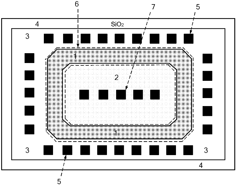
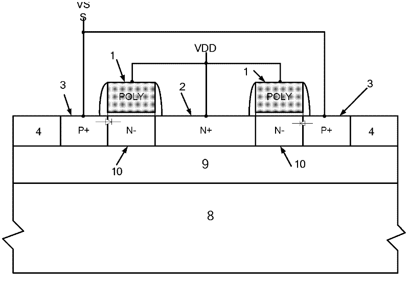
[0018] Such as figure 1 and figure 2 As shown: the ESD protection structure includes an SOI substrate, the SOI substrate includes a substrate 8 , a buried oxide layer 9 is provided on the substrate 8 , and a silicon film is provided on the buried oxide layer 9 . An active area for forming an ESD structure is formed on the silicon film, and an isolation area 4 is provided on the outer periphery of the active area, and the isolation area 4 is silicon dioxide. The active region includes a diffusion region 2 of the first conductivity type, a substrate 10 of the first conductivity type is provided on the outer circumference of the diffusion region 2 of the first conductivity type, and a substrate 10 of the first conductivity type is provided on the outer circumference of the substrate 10 of the first conductivity type. The diffusion region 3 of the second conduct...


PUM

PropertyMeasurementUnit
Lengthaaaaaaaaaa

Abstract

The invention relates to an electrostatic discharge (ESD) protection structure between a silicon-on-insulator (SOI) / CMOS integrated circuit power supply and ground. The ESD protection structure comprises a SOI base plate. The SOI substrate comprises a silicon film. An active region is arranged on the silicon film. An isolation region is arranged on an outer ring of the active region. The active region comprises a first conductive type diffusion area. The outer ring of the first conductive type diffusion area is provided with a first conductive type substrate. The outer ring of the first conductive type substrate is provided with a second conductive type diffusion area. A gate oxide is arranged above the first conductive type substrate. A polysilicon gate is arranged on the gate oxide. The polysilicon gate is in an annular shape. A structure is simple. Technology steps are compatible with a traditional SOI technology and are easy to be realized. A N-type gate control diode structure which is optimized on the technology and a layout is used so as to improve a tolerance level of the ESD between the SOI / CMOS integrated circuit power supply and the ground.

Description

technical field [0001] The invention relates to an ESD protection structure, in particular to an ESD protection structure between an SOI / CMOS integrated circuit power supply and ground, and belongs to the technical field of ESD protection on integrated circuits. Background technique [0002] The full dielectric isolation of components in SOI / CMOS integrated circuits completely eliminates the latch-up effect of bulk silicon circuits, and at the same time has the advantages of small parasitic capacitance, high speed, high integration, wide operating temperature range, and strong radiation resistance, making it It has been mainly used in large-scale integrated circuits of electronic systems in space radiation environments and strategic weapons in strong radiation environments. However, Electrostatic discharge (ESD, Electrostatic discharge) is a major factor affecting the reliability of SOI / CMOS integrated circuits. Due to the different materials and processes for preparing SOI...

Claims


Application Information

Patent Timeline
IPC IPC(8): H01L27/02
Inventor 罗静薛忠杰周昕杰胡永强周毅
Owner 58TH RES INST OF CETC
Learn More