Circuit converting high-voltage power supply into low-voltage power supply for enabling zero switching current of chip

A technology for shutting off current and low-voltage power supply, which is applied in the direction of output power conversion devices, electrical components, and adjustment of electrical variables. Simple circuit structure, stable and reliable control effect

Inactive Publication Date: 2012-02-29
WUXI CHIPOWN MICROELECTRONICS
View PDF8 Cites 8 Cited by
  • Summary
  • Abstract
  • Description
  • Claims
  • Application Information

AI Technical Summary

Problems solved by technology

[0003] There are two current methods to solve this problem. One is to make the chip enable module consume a small quiescent current whether it is in the on state or in the off state, but this method does not meet the requirements of the off quiescent current. The requirement is zero, and in order to make the quiescent current very small, a large resistor needs to be connected in series inside the circuit to limit the quiescent current, which increases the cost of the chip. The advantage of this method is that the work is relatively stable, and the disadvantage is that the performance index is poor. higher cost
The other is to use a special device such as a JFET. Using the device characteristics of the JFET, when the chip is in the off state, the JFET provides a voltage that has been converted from a high voltage to a low voltage power supply to supply power to the internal logic circuit. Since the internal logic circuit is a digital circuit, The digital circuit consumes almost zero current during static operation and can output effective control signals. Therefore, the circuit of the chip enable module with a device architecture such as JFET is simple and convenient to implement. However, since JFET is a special device, the process Realization requires additional lithography, and the device characteristics are difficult to control, and the risk is relatively high

Method used


Image

  • Circuit converting high-voltage power supply into low-voltage power supply for enabling zero switching current of chip
  • Circuit converting high-voltage power supply into low-voltage power supply for enabling zero switching current of chip
  • Circuit converting high-voltage power supply into low-voltage power supply for enabling zero switching current of chip

Examples


Embodiment Construction

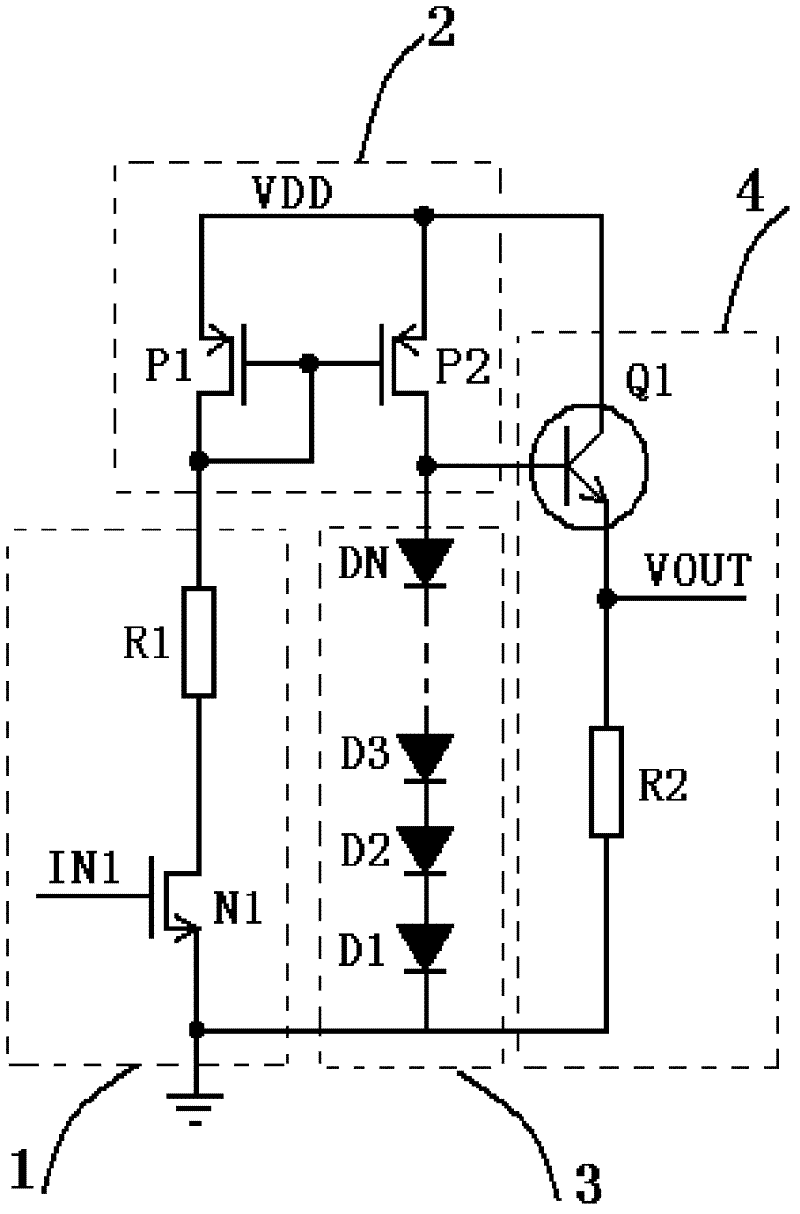
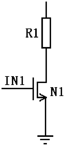
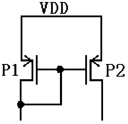
[0019] Such as figure 1 The shown high-voltage to low-voltage power supply circuit for chip enabling zero-off current includes an enabling control circuit 1 , a high-voltage PMOS tube proportional current mirror 2 , a diode series network 3 , and a current amplification output circuit 4 . The enabling control circuit 1 is composed of a high-voltage NMOS transistor N1 and a first resistor R1. The gate terminal of the high-voltage NMOS transistor N1 is connected to the input control signal IN1, the source terminal is grounded, and the drain terminal is connected to one end of the first resistor R1. According to the device characteristics of the NMOS transistor, when the voltage of the control signal IN1 is less than the turn-on voltage VTH of the high-voltage NMOS transistor N1, the high-voltage NMOS transistor N1 is in the cut-off state, and the current flowing through the high-voltage NMOS transistor N1 is zero. When the voltage of the control signal IN1 When it is greater tha...


PUM


Abstract

The invention discloses a circuit converting a high-voltage power supply into a low-voltage power supply for enabling zero switching current of a chip. The circuit comprises an enabling control circuit, a high-voltage PMOS (P-channel Metal Oxide Semiconductor) tube proportion current mirror, a diode series connection network and a current amplifying and outputting circuit. According to the circuit disclosed by the invention, the low-voltage power supply which is converted from the high-voltage power supply and is required by a chip enabling module is realized by directly adopting a general device in a high-voltage process without a special device. The invention has the technical characteristics that: in the circuit disclosed by the invention, the high-voltage power supply is converted into the low-voltage power supply without a traditional architecture consuming quiescent current or the special device; the same function is achieved by adopting the most general device in the high-voltage process, so that the manufacturing cost of the process can be reduced; meanwhile, the quiescent current can be ensured to be zero when the chip is positioned in an enabling switching state; in addition, a low-voltage output power supply has basically no fluctuation along with the change of the high-voltage power supply; and stable voltage output and safety and reliability for work are achieved.

Description

technical field [0001] The invention belongs to integrated circuit chip technology, and in particular relates to a high-voltage-to-low-voltage power supply circuit for chip enabling zero-off current. Background technique [0002] A high-voltage power supply integrated circuit can be divided into a high-voltage power supply module and a low-voltage power supply module. The power supply of the high-voltage power supply module is directly provided by an external high-voltage power supply, and the power supply of the low-voltage power supply module needs to be converted from a high-voltage power supply to a low-voltage power supply. For the entire chip system, the chip enable module is the first module to start to operate. Generally, this module cannot be powered by a low-voltage module, because in terms of power-on sequence, after the chip enable module sends an effective control signal, the high-voltage to low-voltage power supply module just started working. Therefore, it is...

Claims


Application Information

Patent Timeline
Patent Type & Authority Applications(China)
IPC IPC(8): H02M3/155H02M1/08
Inventor 张立新邹宇彤陈健易扬波周飙李海松张韬
Owner WUXI CHIPOWN MICROELECTRONICS
Why Eureka
Try Eureka