

High-efficient GaN-based semiconductor light emitting diode
A technology of light-emitting diodes and semiconductors, applied in semiconductor devices, electrical components, circuits, etc., to achieve the effects of improving luminous efficiency, reducing electron leakage current, and increasing electron concentration
- Summary
- Abstract
- Description
- Claims
- Application Information
AI Technical Summary
Problems solved by technology
Method used
Image

Examples
Embodiment Construction
[0018] The present invention will be further described in detail below through the embodiments and accompanying drawings.
[0019] Implementation process one
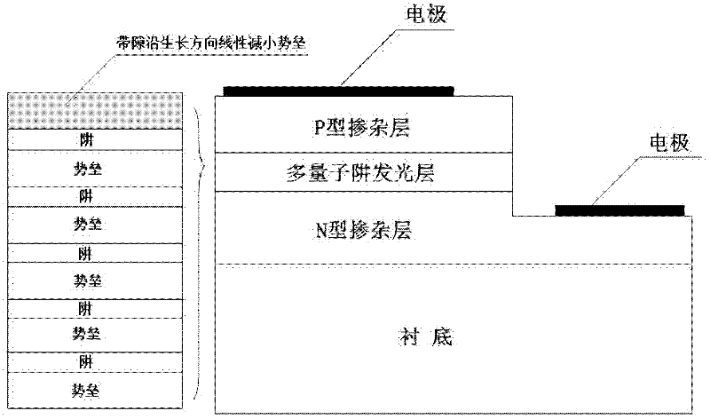
[0020] The present invention consists of a substrate, an N-type doped layer, a multi-quantum well light-emitting layer, a P-type doped layer and an electrode, and its structure is as follows: figure 1 shown.
[0021] The substrate material is sapphire, silicon or silicon carbide.
[0022] The N-type doped layer is a silicon-doped GaN-based semiconductor material, which can be GaN, AlGaN or InGaN, and the doping concentration is 1×10 17 ~1×10 20 cm -3 .
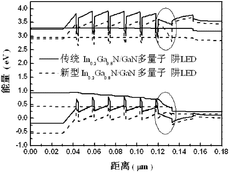
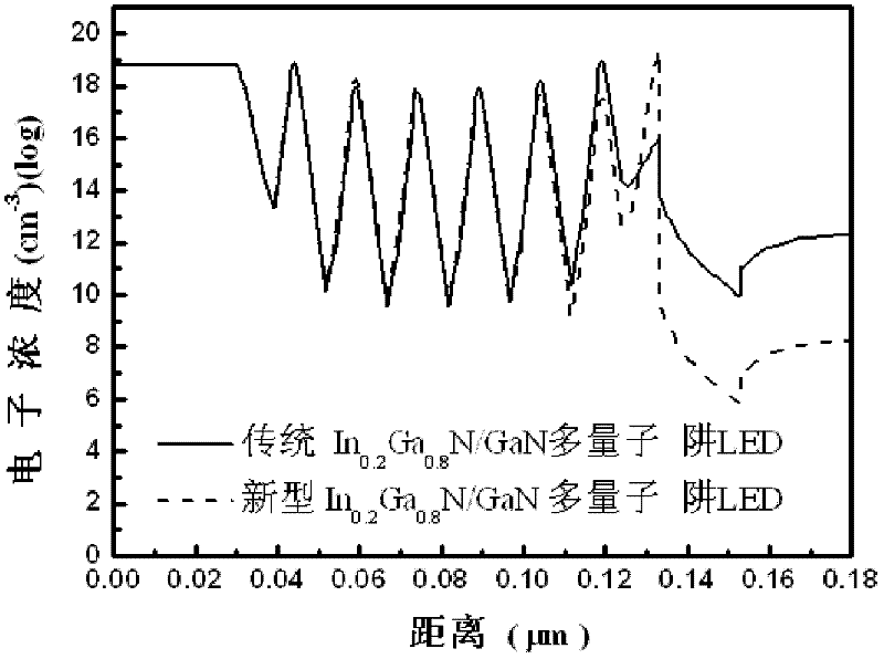
[0023] The multi-quantum well light-emitting layer is an InGaN / GaN multi-quantum well structure, or an InGaN / InGaN multi-quantum well structure, or a GaN / AlGaN multi-quantum well structure, or an AlGaN / AlGaN multi-quantum well structure; the multi-quantum well structure is close to P The bandgap of the last potential barrier of the type AlGaN electron blocking lay...
PUM
| Property | Measurement | Unit |
|---|---|---|
| Doping concentration | aaaaa | aaaaa |
Abstract
Description
Claims
Application Information