Ion-implanted one-dimensional electron gas GaN-based HEMT (high electron mobility transistor) device and preparation method

An ion implantation and electron gas technology, applied in the field of microelectronics, can solve the problems of small breakdown electric field, high carrier concentration, limited electron concentration, etc., and achieve high temperature and high pressure characteristics, high electron mobility, and improved power characteristics. Effect

Active Publication Date: 2013-10-23
陕西半导体先导技术中心有限公司
View PDF6 Cites 4 Cited by
  • Summary
  • Abstract
  • Description
  • Claims
  • Application Information

AI Technical Summary

Problems solved by technology

[0017] one. Due to the small bandgap of Si and GaAs semiconductor materials, the intrinsic carrier concentration is high and the breakdown electric field is small, which makes the prepared Si-based and GaAs-based devices have poor high-temperature and high-voltage characteristics and poor radiation resistance. weak;
[0018] two. Due to the poor electron transport characteristics of Si and GaAs semiconductor materials, the frequency characteristics of Si-based and GaAs-based devices prepared are poor;
[0019] three. Due to the poor polarization characteristics of Si and GaAs semiconductor materials when forming heterojunctions, the electron concentration is greatly limited, making the prepared Si-based and GaAs-based devices have poor power characteristics.

Method used


Image

  • Ion-implanted one-dimensional electron gas GaN-based HEMT (high electron mobility transistor) device and preparation method
  • Ion-implanted one-dimensional electron gas GaN-based HEMT (high electron mobility transistor) device and preparation method
  • Ion-implanted one-dimensional electron gas GaN-based HEMT (high electron mobility transistor) device and preparation method

Examples


Embodiment 1

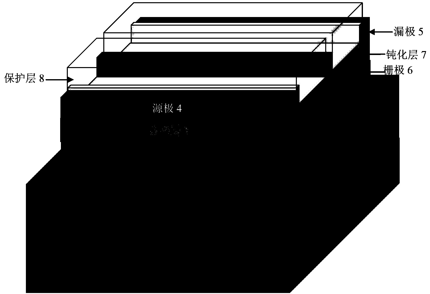
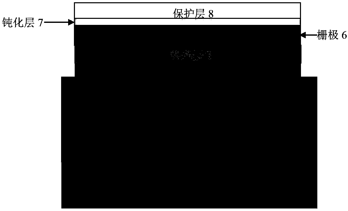
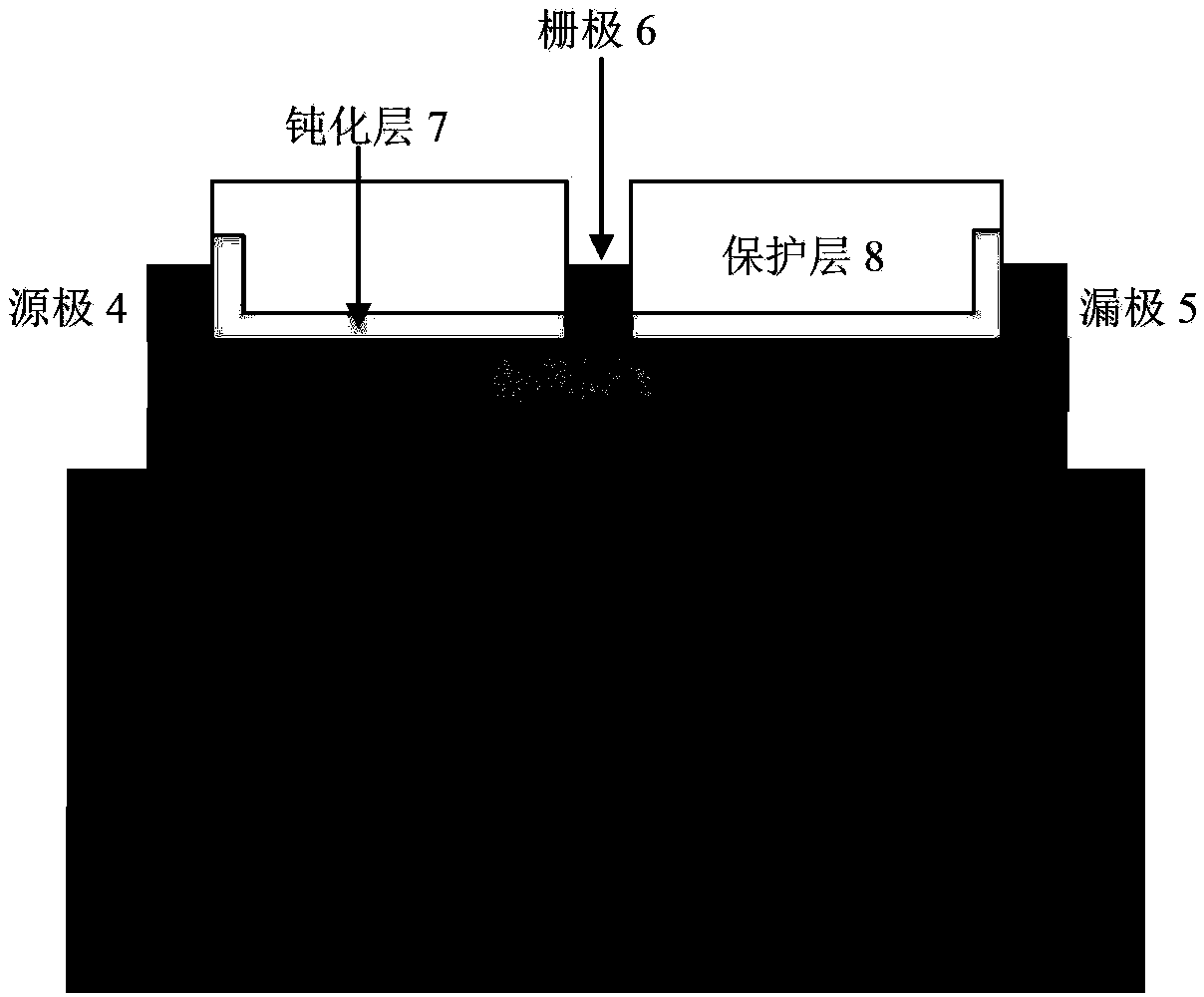
[0054] Embodiment 1, the production substrate 1 is sapphire, the buffer layer 2 is GaN, the barrier layer 3 is AlGaN, the passivation layer 7 is SiN, the protective layer 8 is SiN, the width of the ion implantation region is 50nm, and the ion implantation region is not A one-dimensional electron gas GaN-based HEMT device with a width of 10 nm, and the ion-implanted region and the non-ion-implanted region are periodically arranged.

[0055] Step 1, using metal organic chemical vapor deposition technology MOCVD to epitaxially GaN semiconductor material with a thickness of 1 μm on the sapphire substrate 1 as the buffer layer 2; the process conditions for the epitaxial GaN buffer layer 2 are: the temperature is 1040 ° C, and the pressure is 200 Torr , the hydrogen flow rate is 4700 sccm, the ammonia gas flow rate is 4700 sccm, and the gallium source flow rate is 200 μmol / min.

[0056] Step 2: Deposit an AlGaN semiconductor material with a thickness of 10 nm on the buffer layer 2 b...

Embodiment 2

[0073] Embodiment 2, the production substrate 1 is silicon carbide, the buffer layer 2 is GaN, the barrier layer 3 is AlGaN, the passivation layer 7 is SiN, and the protective layer 8 is SiO 2 , the width of the ion-implanted region is 250nm, the width of the non-ion-implanted region is 50nm, and the ion-implanted region and the non-ion-implanted region are periodically arranged one-dimensional electron gas GaN-based HEMT devices.

[0074] Step 1, epitaxially epitaxially GaN buffer layer 2 with a thickness of 3 μm on silicon carbide substrate 1 .

[0075] Using metal-organic chemical vapor deposition MOCVD equipment, under the process conditions of temperature 1060 ° C, pressure 200 Torr, hydrogen flow rate 4900 sccm, ammonia gas flow rate 4900 sccm, gallium source flow rate 210 μmol / min, on a silicon carbide substrate 1 A GaN buffer layer 2 with a thickness of 3 μm is epitaxially formed.

[0076] Step 2, depositing an AlGaN barrier layer 3 with a thickness of 30 nm on the Ga...

Embodiment 3

[0100] Embodiment 3, the production substrate 1 is silicon, the buffer layer 2 is GaN, the barrier layer 3 is AlGaN, and the passivation layer 7 is SiO 2 , the protective layer 8 is SiN, the width of the ion-implanted region is 500nm, and the width of the non-ion-implanted region is 100nm, and the ion-implanted region and the non-ion-implanted region are periodically arranged one-dimensional electron gas GaN-based HEMT devices.

[0101] In step A, a GaN buffer layer 2 with a thickness of 5 μm is epitaxially formed on the silicon substrate 1 .

[0102] A GaN buffer layer 2 with a thickness of 5 μm was epitaxially grown on a silicon substrate 1 using metal-organic chemical vapor deposition MOCVD equipment; The gas flow rate is 5200 sccm, and the gallium source flow rate is 220 μmol / min.

[0103] Step B, depositing an AlGaN barrier layer 3 with a thickness of 50 nm on the GaN buffer layer 2 .

[0104]Metal-organic chemical vapor deposition MOCVD equipment is used to deposit an ...


PUM


Abstract

The invention discloses an ion-implanted one-dimensional electron gas GaN-based HEMT (high electron mobility transistor) device and a preparation method. The problems of poorer high-temperature high-voltage characteristics, frequency characteristics and power characteristics of the conventional one-dimensional electron gas device are mainly solved. The device comprises a substrate, buffer layer, a potential barrier layer, a passivation layer and a protective layer from bottom to top, wherein a source and a drain are arranged at two ends on the potential barrier layer respectively; the passivation layer is positioned on the potential barrier layer between the source and the drain; a gate trough is formed in the passivation layer, and a gate is arranged in the gate trough; the buffer layer is made from GaN, and the potential barrier layer is made from AlGaN; anions are implanted into local areas on the potential barrier layer, and the areas where the anions are implanted are a plurality of spaced strips; the widths of areas where the anions are not implanted between the strips are at a nanometer order of magnitude, and a one-dimensional electron gas is formed in heterogeneous junctions below the areas where the anions are implanted. Compared with Si-based and GaAs-based devices, the device has good high-temperature high-voltage characteristics, good frequency characteristics and good power characteristics, and a one-dimensional electron gas device with super-high speed and low power consumption can be manufactured.

Description

technical field [0001] The invention belongs to the technical field of microelectronics and relates to a semiconductor device, in particular a one-dimensional electron gas HEMT device based on a GaN semiconductor material heterojunction structure, which can be used as a basic device of a microwave, millimeter wave communication system and a radar system. Background technique [0002] III-V compound semiconductor materials are the third-generation semiconductor materials that have been developed rapidly for more than ten years, such as GaN-based, GaAs-based, InP-based and other semiconductor materials, which have a large band gap and can be combined with InN, AlN, etc. Alloy semiconductors are formed to make their forbidden band width adjustable. People usually use these III-V compound semiconductor materials to form various heterojunction structures. Due to the large difference in the forbidden band width of the III-V compound semiconductor materials on both sides of the het...

Claims


Application Information

Patent Timeline
Patent Type & Authority Applications(China)
IPC IPC(8): H01L29/775H01L29/20H01L29/205H01L21/335H01L21/266
Inventor 马晓华汤国平郝跃陈伟伟赵胜雷
Owner 陕西半导体先导技术中心有限公司
Why Eureka
Try Eureka