Method and device for manufacturing micro-fluidic chip with femtosecond plasma grating

A microfluidic chip and plasma technology, which is applied in the manufacture of microstructure devices, microstructure devices, manufacturing tools, etc., can solve the problems that are not conducive to femtosecond laser fine processing and reduce processing efficiency, so as to reduce production time and increase The effect of movement speed

Active Publication Date: 2020-07-14
CHONGQING INST OF EAST CHINA NORMAL UNIV +1
View PDF16 Cites 3 Cited by
  • Summary
  • Abstract
  • Description
  • Claims
  • Application Information

AI Technical Summary

Problems solved by technology

[0004] Chinese patent document CN 101101356A describes that the use of femtosecond lasers can effectively process microfluidic optical waveguides on quartz glass substrates. However, in this method, sputtered particles are easily attached to the objective lens during processing

Method used


Image

  • Method and device for manufacturing micro-fluidic chip with femtosecond plasma grating
  • Method and device for manufacturing micro-fluidic chip with femtosecond plasma grating
  • Method and device for manufacturing micro-fluidic chip with femtosecond plasma grating

Examples


Embodiment 1

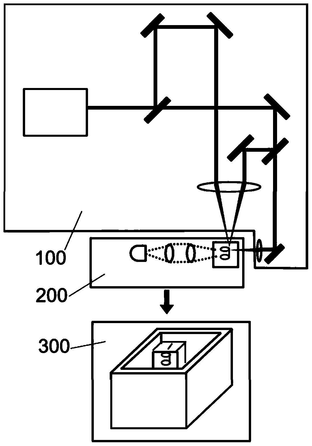
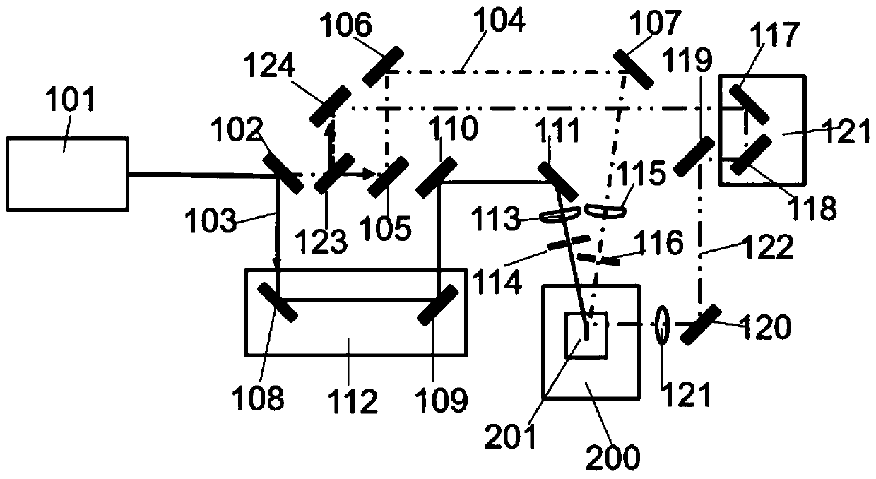
[0035] See attached figure 2 , the femtosecond pulsed laser output by the femtosecond pulsed laser 101 in the plasma grating optical path 100 is divided into after passing through the plane beam splitter 102 which reflects 30% and transmits 70% and the beam splitting ratio is one to one plane beam splitter 102. First reflected beam 103 at 30% power, second reflected beam 122 at 35% power and transmitted beam 104 at 35% power. The first time domain delay controller is made up of the 4th plane mirror 108, the 5th plane mirror 109 and displacement platform 112, and the second time domain delay controller is made up of the 9th plane mirror 117, the 10th plane mirror 118 and displacement The platform 121 is composed. The first reflected light beam 103 changes the optical path through the sixth plane mirror 110 and the seventh plane mirror 111 after passing through the first time domain delay controller, and converges after passing through the first plano-convex cylindrical lens 1...


PUM


Abstract

The invention discloses a method and device for manufacturing a micro-fluidic chip with a femtosecond plasma grating. The method is characterized in that two or more beams of femtosecond pulse lasersact on quartz glass together at a certain included angle and converge in the quartz glass, and when pulses achieve synchronization in time domain, pulses of two beams of light interfere; under the constraint of an interference field, only one filament is formed in a place where interference is constructive; and multiple filaments are arranged equidistantly in space to form the plasma grating; andthe device for manufacturing the micro-fluidic chip comprises a plasma grating light path, a micro-channel processing platform and a hydrofluoric acid ultrasonic pool. Compared with the prior art, themethod and the device have the advantages of increasing the manufacturing speed of the quartz glass micro-fluidic chip and improving the roughness quality of a micro-channel wall surface; especiallythe micro-fluidic chip of a three-dimensional structure can be conveniently processed; a new preparation method is provided for manufacturing of micro-channel chips, and the new preparation has uniqueadvantages especially in processing the micro-fluidic chip with an ultrafast optical technology.

Description

technical field [0001] The invention relates to the technical field of microchannel chip manufacturing, in particular to a microfluidic chip and a device thereof manufactured by using a femtosecond plasma grating. Background technique [0002] The microfluidic chip based on microfluidic technology can integrate sample collection, transfer, dilution, reaction, separation, detection and other functions on micro-scale materials. The consumption of reagents is therefore widely used in medicine, biology, chemistry, materials, etc. and their cross fields. The structure of the microchannel in the microfluidic chip is individually designed according to the application requirements, and consists of various independent microchannels and conduits between the microchannels. With the development of microfluidic technology, highly integrated and highly automated microfluidic chips are becoming increasingly important in biochemical reaction experiments. [0003] At present, the manufactu...

Claims


Application Information

Patent Timeline
IPC IPC(8): B23K26/55B23K26/064B23K26/03B23K26/067B01L3/00
CPCB23K26/55B23K26/064B23K26/0643B23K26/0648B23K26/032B23K26/0676B01L3/5027B01L2200/10B23K2103/54B23K26/53B23K26/0624B23K2103/00B23K26/0006B23K26/0861B81C1/00071B81C1/00531B81C1/00539B81C2201/0132B81C2201/0133B81C2201/0143B81C2900/00G01J3/26G02B26/001
Inventor 曾和平南君义胡梦云闫明
Owner CHONGQING INST OF EAST CHINA NORMAL UNIV
Why Eureka
Try Eureka