Method for etching metal tungsten material

A metal tungsten, dry etching technology, applied in metal material coating process, process for producing decorative surface effects, coating and other directions, can solve the problems of low etching process rate and poor anisotropy

Active Publication Date: 2012-03-14
苏州含光微纳科技有限公司
View PDF4 Cites 14 Cited by
  • Summary
  • Abstract
  • Description
  • Claims
  • Application Information

AI Technical Summary

Problems solved by technology

[0005] At present, there is no relevant report on MEMS devices fabricated using metal tungsten body materials as the main structure, and the etching process rate of existing thin-film tungsten materials is generally low and the anisotropy is poor, which has become the main bottleneck
It is suitable for the processing of metal tungsten materials, and there is no report on the etching process that can realize high-speed, high-aspect-ratio etching

Method used


Image

  • Method for etching metal tungsten material
  • Method for etching metal tungsten material
  • Method for etching metal tungsten material

Examples


Embodiment Construction

[0019] The following examples will further illustrate the present invention, but this is not a limitation of the present invention. Those skilled in the art can make various modifications or improvements based on the basic idea of ​​the present invention, but they are all available as long as they do not deviate from the basic idea of ​​the present invention. Within the scope of the present invention.

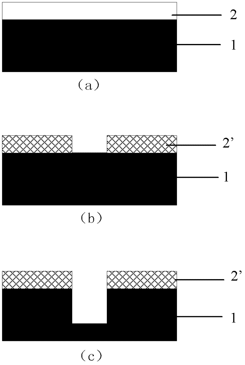
[0020] 1. Preparation of etching mask:

[0021] Such as figure 1 As shown, the negative photoresist SU-83050 is used as the mask material, and the polished high-purity wafer-grade metal tungsten substrate 1 is cleaned with acetone alcohol and dried, and then coated with a layer of Negative photoresist 2 with a thickness of 60 microns, such as figure 1 (a) Shown. After the photoresist 2 is patterned by pre-baking, exposure, post-baking, and developing, an etching mask 2'with the required etching pattern is obtained, see figure 1 (b).
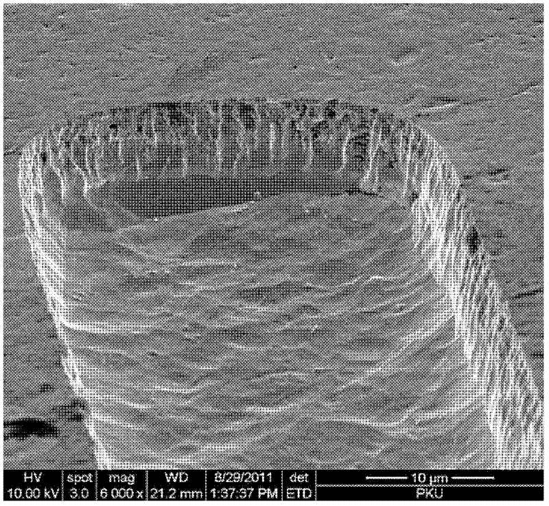
[0022] 2. Etching:

[0023] Use Trion Technology ...


PUM

PropertyMeasurementUnit
thicknessaaaaaaaaaa
thicknessaaaaaaaaaa

Abstract

The invention discloses a method for etching a metal tungsten material, which is characterized in that: an etching mask is formed on the metal tungsten material, and then a high-density plasma (such as inductively coupled plasma, transformer coupled plasma and the like) dry etching process is adopted to produce high-density and high-energy ions and free radicals and to realize the high-speed and anisotropic etching of the metal tungsten material. The etching speed can reach 2.95 micrometers per minute, and the verticality of an etching-resulted side wall can reach 60 degrees. Based on the method, a metal tungsten underlay substrate can be used as a main body material for preparing micro-electro-mechanical system (MEMS) devices.

Description

Technical field [0001] The invention belongs to the technical field of microelectronic mechanical systems (MEMS) technology, and particularly relates to an anisotropic, high-speed dry etching method for metal tungsten body materials. Background technique [0002] In the processing and manufacturing of MEMS devices, traditional structural substrate materials usually use single crystal silicon materials, but single crystal silicon materials have some inherent defects, such as high brittleness and poor impact resistance; relatively metal materials have poor conductivity and have the same resistivity. High; thermal stability is relatively poor, and Young's modulus will change significantly when it exceeds 600°C, which is not suitable for application under high temperature conditions, which affects the application range of the device. [0003] Metal tungsten material is the metal with the highest melting point in nature (3410℃), and it also has the characteristics of high strength, high...

Claims


Application Information

Patent Timeline
Patent Type & Authority Applications(China)
IPC IPC(8): B81C1/00
Inventor 陈兢胡佳张轶铭陈书慧李男男李天宇
Owner 苏州含光微纳科技有限公司
Why Eureka
Try Eureka