
Infrared focal plane array device and manufacture method thereof

A technology of an infrared focal plane and a manufacturing method, which is applied in the field of infrared focal plane array devices and their manufacturing, can solve the problems of incompatibility of VOx materials, inability to dissipate infrared energy in time, and high device cost, so as to improve the quality of infrared imaging and increase the Thermal isolation effect, effect of improving absorption efficiency

Active Publication Date: 2012-03-21
北京中科微投资管理有限责任公司
View PDF4 Cites 12 Cited by
  • Summary
  • Abstract
  • Description
  • Claims
  • Application Information

AI Technical Summary

Problems solved by technology

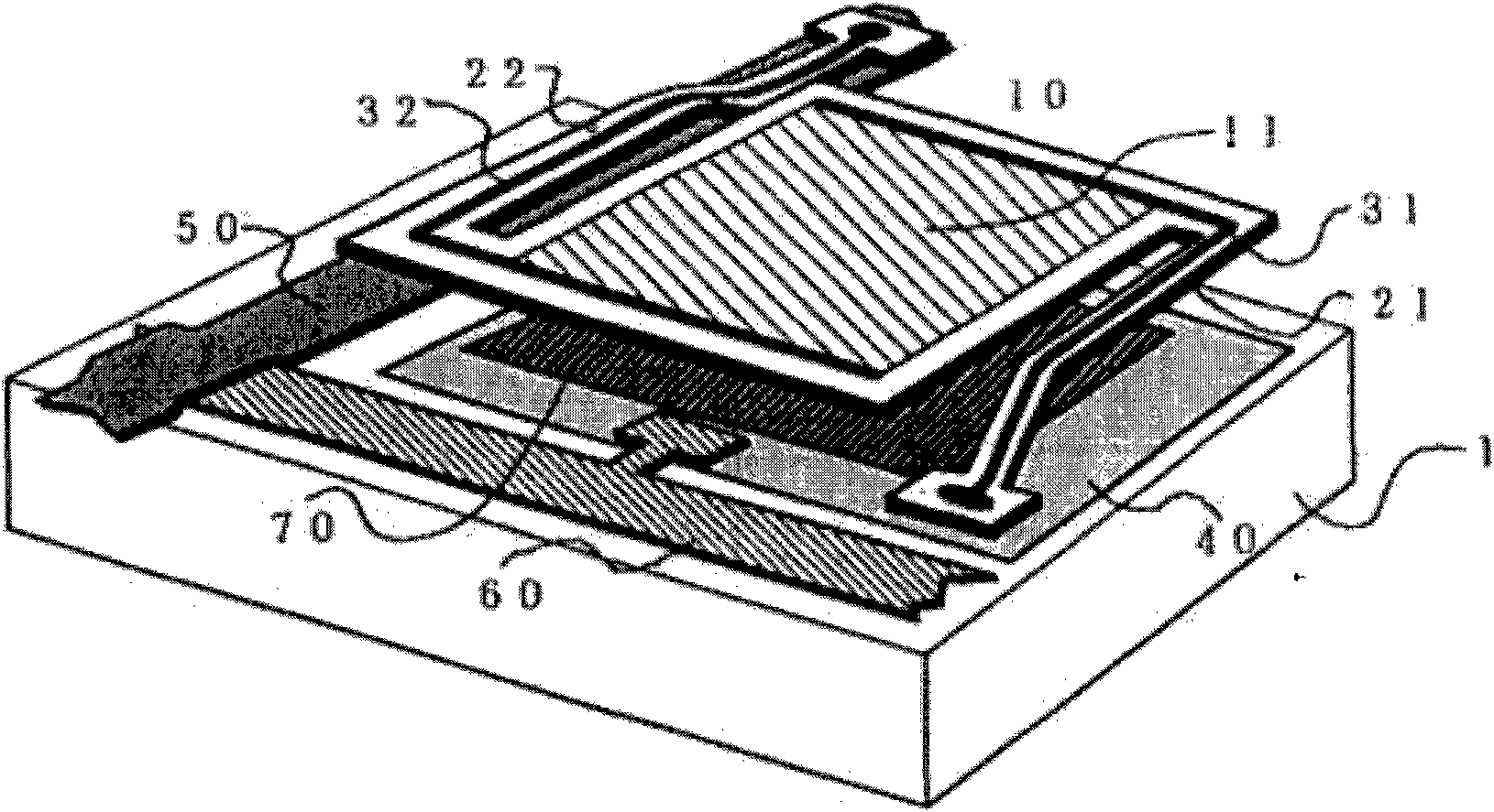
[0006] Since the production of VOx materials cannot be compatible with the conventional IC process, the infrared focal plane array device with the above structure cannot be mass-produced in the existing integrated circuit manufacturing plant, resulting in relatively high device cost, which affects its popularization and application.
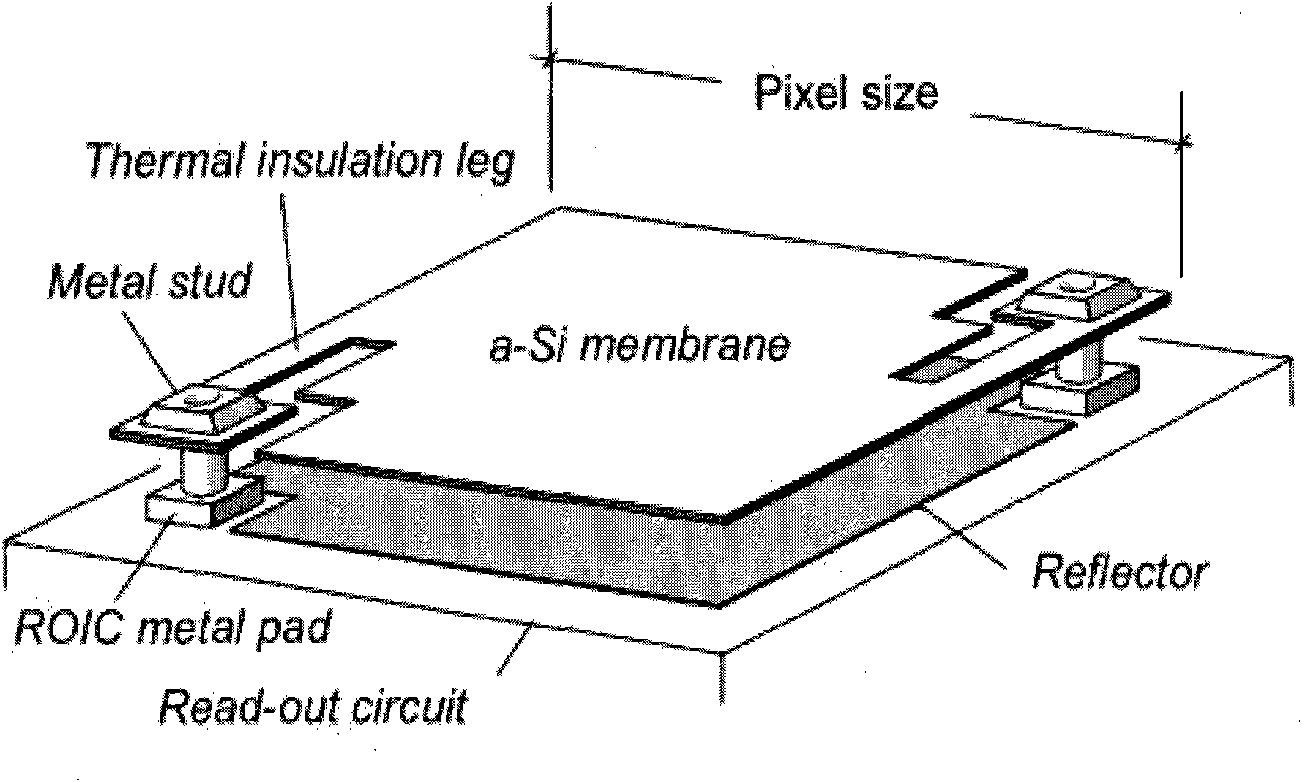
In addition, both of the above two structures are manufactured on the silicon chip with the readout circuit already formed. Generally, the silicon chip with the readout circuit has a thicker dielectric layer, thus forming a larger heat capacity, and the infrared energy absorbed by the detection unit Failure to dissipate in time will lead to crosstalk between multiple detection units, thereby reducing the quality of infrared imaging

Method used


Image

  • Infrared focal plane array device and manufacture method thereof
  • Infrared focal plane array device and manufacture method thereof
  • Infrared focal plane array device and manufacture method thereof

Examples


Embodiment 1

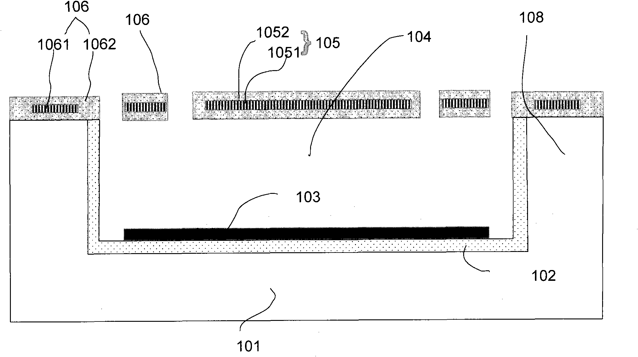
[0056] image 3 It is a schematic structural diagram of the infrared focal plane array device in this embodiment, Figure 4 for image 3 In order to clearly show the innovation of the present invention, only one detection unit of the infrared focal plane array is shown in the figure, and the detection unit includes:

[0057] Substrate 101;

[0058] a cavity 104 located in the substrate 101;

[0059] an infrared sensitive layer 105 suspended above the cavity 104;

[0060] A reflective layer 103, disposed at the bottom of the cavity 104, opposite to the infrared sensitive layer 105;

[0061] The cantilever beam 106 is suspended above the substrate 101 and is substantially at the same level as the infrared sensitive layer 105 , one end of which is fixedly connected to the substrate 101 , and the other end is fixedly connected to the infrared sensitive layer 105 .

[0062] Wherein, the substrate 101 is a bare wafer of single crystal silicon, and the cavity 104 is formed by etch...

Embodiment 2

[0076] Figure 10 It is a schematic structural diagram of the infrared focal plane array device in this embodiment. Similarly, its detection unit also includes: a substrate 201, a cavity 204 located in the substrate 201, suspended above the cavity 204 The infrared sensitive layer 205 is arranged on the bottom of the cavity 204, opposite to the infrared sensitive layer 205, the reflective layer 203 is suspended on the cantilever beam 206 above the substrate 201, and one end of the cantilever beam is fixed to the heat sink 208 connected, and the other end is fixedly connected with the infrared sensitive layer 205.

[0077] The difference from the first embodiment is that the heat sink 208 is formed on the surface of the substrate, and the cavity 204 is surrounded by the heat sink 208 . In other words, the heat sink 208 is not integrated with the substrate 201 , but is a specially formed structure on the surface of the substrate, and the cavity 204 is not formed by etching the s...

Embodiment 3

[0086] Figure 16 It is a schematic structural diagram of the infrared focal plane array device in this embodiment, Figure 17 for Figure 16 The top view of the figure shows only one detection unit, Figure 18 for Figure 17 Schematic diagram of the detection cell array.

[0087] Such as Figure 16 , 17 As shown, the difference from the previous embodiments is that the cantilever beam 306 is disposed above the heat sink 308 around the cavity 304 , with a gap between the cantilever beam 308 and the heat sink 308 . An anchor 309 is used to connect one end of the cantilever beam 306 to the heat sink and the other end to the infrared sensitive layer 305 to support the entire infrared sensitive layer. In this way, the infrared sensitive layer 305 can cover almost the entire upper area of ​​the cavity 304 , which increases the effective reflection area of ​​the resonant absorption structure, thereby improving the absorption efficiency of the infrared sensitive layer 305 .

...


PUM


Abstract

The invention provides an infrared focal plane array device, which comprises a substrate, a cavity, an infrared sensing layer, a reflecting layer and a cantilever beam, wherein the cavity is positioned in the substrate, the infrared sensing layer is suspended above the cavity, the reflecting layer is arranged at the bottom of the cavity and is opposite to the infrared sensing layer, the cantilever beam is suspended above the substrate, one end of the cantilever beam is fixedly connected with the substrate, the other end of the cantilever beam is fixedly connected with the infrared sensing layer, the substrate around the cavity is a heat sinking element for heat radiation, and the end of the cantilever beam connected with the substrate is connected onto the heat sinking element. Correspondingly, the invention also provides a manufacture method of the infrared focal plane array device. The infrared focal plane array device adopts a resonance absorption structure consisting of the reflecting layer, the infrared sensing layer and the cavity formed between the two layers for improving the absorption efficiency of a detection unit on infrared rays, and the manufacture of the resonance absorption structure is completely compatible with the conventional integrated circuit (IC) process.

Description

technical field [0001] The invention relates to the technical field of infrared imaging, in particular to an infrared focal plane array device and a manufacturing method thereof. Background technique [0002] Infrared imaging technology is widely used in military, industrial, agricultural, medical, forest fire prevention, environmental protection and other fields. The core component of infrared imaging device is Infrared Focal Plane Array (IRFPA). According to the classification of working principle, infrared imaging devices can be divided into: photon infrared detectors and uncooled infrared detectors. [0003] Photon-type infrared detectors use narrow bandgap semiconductor materials, such as HgCdTe, InSb, etc., and use the photoelectric effect to realize the conversion of infrared light signals into electrical signals. Therefore, to work at a temperature of 77K or lower, this requires a heavy and Complex refrigeration equipment makes it difficult to miniaturize this infra...

Claims


Application Information

Patent Timeline
IPC IPC(8): G01J5/10
Inventor 欧文刘战峰陈大鹏
Owner 北京中科微投资管理有限责任公司
Learn More