Microstrip bimodule band-pass filter based on DGS (defected ground structure) square-ring resonator

A ring resonator and filter technology, applied in waveguide devices, electrical components, circuits, etc., can solve problems such as difficult external coupling and bandwidth limitation, and achieve the effects of expanding bandwidth, increasing stopband bandwidth, and reducing resonance frequency

Inactive Publication Date: 2014-06-04
XIDIAN UNIV
View PDF3 Cites 1 Cited by
  • Summary
  • Abstract
  • Description
  • Claims
  • Application Information

AI Technical Summary

Problems solved by technology

However, this technique is only applicable to the case of symmetrical frequency response, and the microstrip square ring resonator using the microstrip feeder slot coupling is not easy to achieve strong external coupling, so the bandwidth is limited

Method used


Image

  • Microstrip bimodule band-pass filter based on DGS (defected ground structure) square-ring resonator
  • Microstrip bimodule band-pass filter based on DGS (defected ground structure) square-ring resonator
  • Microstrip bimodule band-pass filter based on DGS (defected ground structure) square-ring resonator

Examples


Embodiment 1

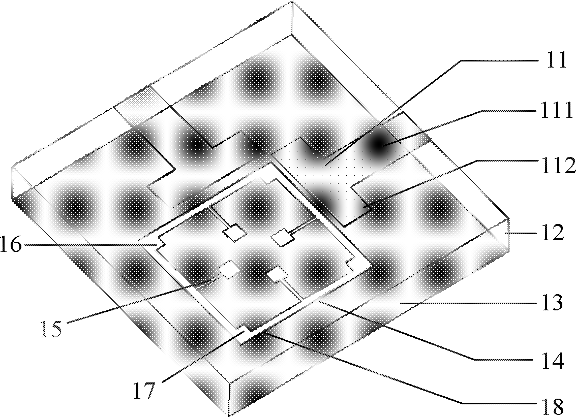
[0038] Reference figure 1 with Figure 4 The present invention is mainly composed of a pair of input and output "T"-shaped feeders 11, a microstrip dielectric substrate 12 and a DGS square ring resonator 18. among them:

[0039] The microstrip dielectric substrate 12 uses a double-sided copper-clad dielectric substrate with a dielectric constant of 9.6 and a thickness of 0.8 mm.

[0040] The DGS square ring resonator 18 is etched on the metal ground plate 13 under the microstrip dielectric substrate 12, and is composed of a square ring 14, four square step impedance branches 15 and four square patches 16. Side length of square ring 24 L 1 =10mm, equal to one-fourth of the waveguide wavelength, corresponding to the resonance frequency ε e Is the effective dielectric constant of the gap microstrip line, the width w of the square ring 24 2 =0.5mm; four square step impedance stubs 15 are etched in the middle of the four sides of the square ring 14, which is defined by the length L 2 ...

Embodiment 2

[0044] Reference figure 1 with Figure 4 The other features of this embodiment are the same as the first embodiment except for the following features: perturbation patch 17 side length p=0.1mm, reference patch side length r=1.7mm, port connection feeder 111 width w=0.8mm, coupling feeder 112 Length L 3 =7mm, width w 3 = 1mm, the relative distance d between the inner side of the coupled feeder and the outer side of the square ring = 0.5mm.

[0045] In the present invention, due to the relatively long distance between the two input and output "T"-shaped feeders 11, the source and load coupling is weak, and there is a transmission zero point on each side of the passband, and a symmetrical filter frequency response is realized, such as Figure 8 As shown, Figure 8 Middle|S 21 | Is the transmission characteristic curve of the filter, |S 11 | Is the reflection characteristic curve of the filter 1 port. by Figure 8 It can be seen that the filter has a symmetrical band-pass frequency r...

Embodiment 3

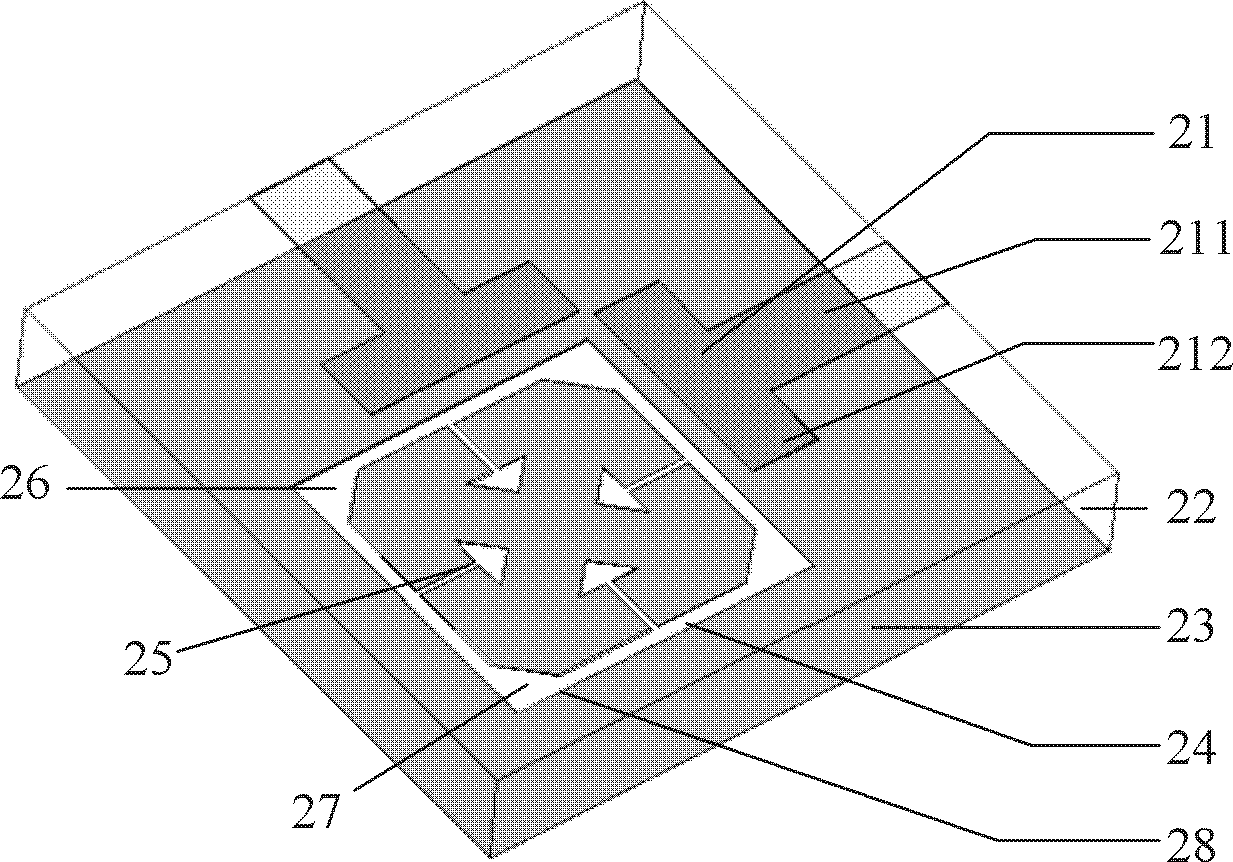
[0047] Reference figure 2 with Figure 5 The present invention is mainly composed of a pair of input and output "T"-shaped feeders 21, a microstrip dielectric substrate 22 and a DGS square ring resonator 28. among them:

[0048] The microstrip dielectric substrate 22 adopts a double-sided copper-clad dielectric substrate with a dielectric constant of 9.6 and a thickness of 0.8 mm.

[0049] The DGS square ring resonator 28 is etched on the metal ground plate 23 under the microstrip dielectric substrate 22, and is composed of a square ring 24, four triangular stepped impedance stubs 25 and four triangular patches 26. Side length of square ring 24 L 1 =10mm, equal to one quarter of the waveguide wavelength, corresponding to the resonance frequency ε e Is the effective dielectric constant of the gap microstrip line, the width w of the square ring 24 1 =1mm; four triangular stepped impedance stubs 25 are etched in the middle of the four sides of the square ring 24, by the length L 2 =...


PUM


Abstract

The invention discloses a microstrip bimodule band-pass filter based on a DGS (defected ground structure) square-ring resonator, in order to mainly solve the problems that the traditional microstrip bimodule filter is narrower in band width, and the transmission zero is difficult to control. The filter comprises a pair of an input / output 'T'-shaped feeder lines (11), a microstrip medium substrate (12) and a square bimodule resonator (18), wherein a square ring (14) is etched on a metal grounding plate (13) below the microstrip medium substrate (12); each step impedance branch knot (15) is etched at the middle parts of the four edges of the square ring; each paster (16) is etched in the four corners of the square ring (16), thus a DGS square ring bimodule resonator (18) is formed. The pair of the input / output 'T'-shaped feeder lines (11) is vertically placed above the microstrip medium substrate with each other, and extends into the resonator in parallel for power feed. According to the invention, external coupling can be intensified, band width can be expanded, symmetrical and unsymmetrical high-inhibition band pass filter frequency response is realized, and the filter can be used for wireless communication systems.

Description

Technical field [0001] The invention belongs to a microstrip device, relates to a microstrip dual-mode bandpass filter, and can be used in a radio frequency front end of a wireless communication system. Background technique [0002] With the rapid development of mobile communications, satellite communications, radar, and remote sensing technologies, the wireless spectrum is becoming increasingly crowded, which places very demanding requirements on radio frequency microwave filters in communication systems. Microstrip filters have the advantages of small size, light weight, low cost, and easy processing, and are widely used in microwave circuits. There are many types and implementations of microstrip filters, and the research on miniaturized high-performance microstrip filters has always been a hot field. Traditional filter forms such as Butterworth and Chebyshev filters can only meet high selectivity requirements by increasing the number of filter stages. The processed filters a...

Claims


Application Information

Patent Timeline
Patent Type & Authority Patents(China)
IPC IPC(8): H01P1/212
Inventor 吴边苏涛张永亮付森梁昌洪
Owner XIDIAN UNIV
Why Eureka
Try Eureka