Air leakage detecting method for reaction cavity and control method for vacuum reactor

A detection method and reaction chamber technology, applied in semiconductor/solid-state device manufacturing, instruments, measuring devices, etc., can solve the problems of processing system capacity impact, reducing production capacity, reducing the processing time of semiconductor processing equipment, etc.

CN102403191BActive Publication Date: 2014-05-21ADVANCED MICRO FAB EQUIP INC CHINA
7 Cites 0 Cited by

Patent Information

Authority / Receiving Office
CN · China
Patent Type
Patents(China)
Current Assignee / Owner
Publication Date
2014-05-21

Smart Images

  • Figure 1
    Figure 1
  • Figure 2
    Figure 2
  • Figure 3
    Figure 3
Patent Text Reader

Abstract

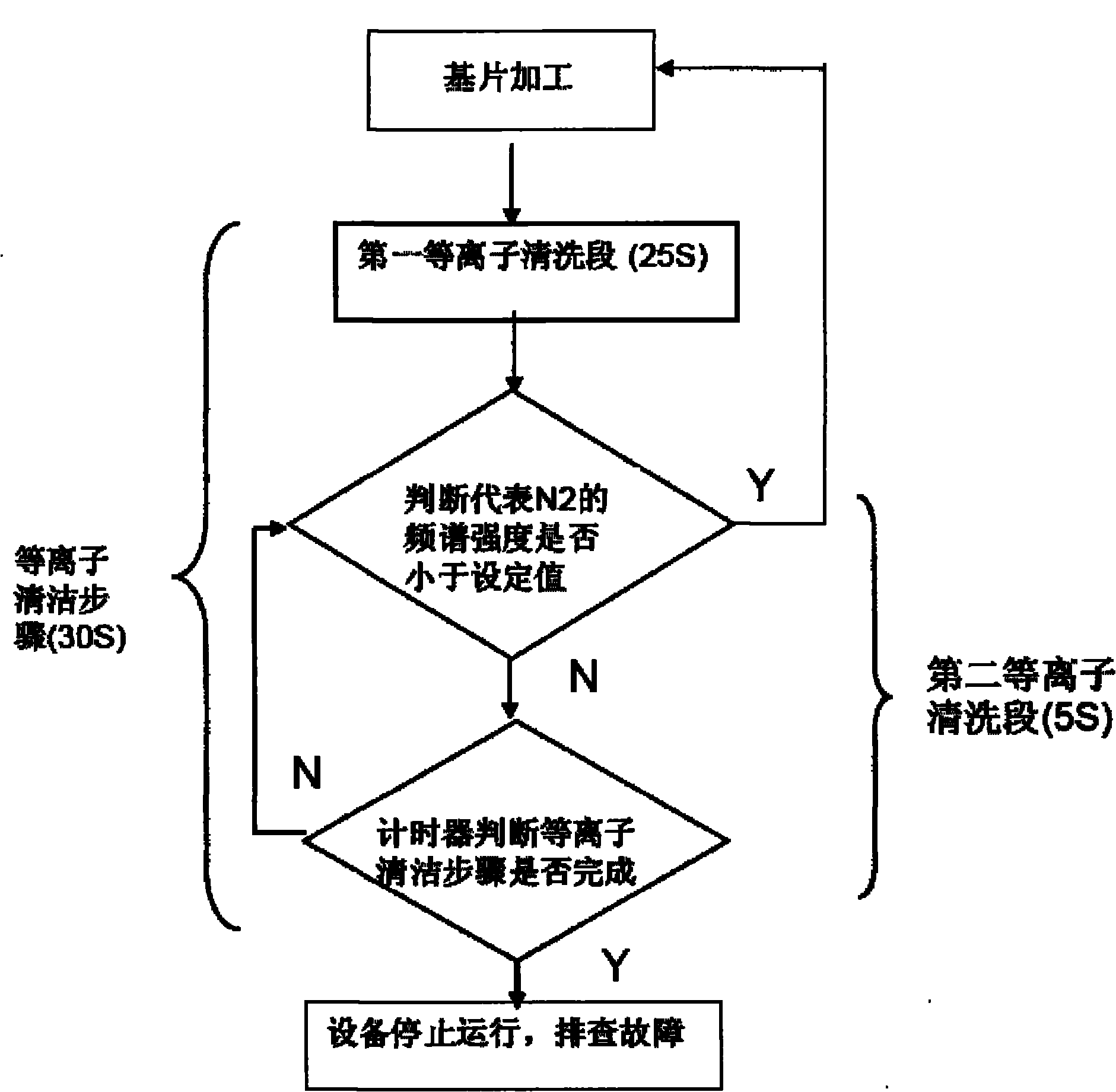
Provided are a kind of reaction chamber air-leakage detection method and a vacuum reactor control method, which is to realize a real-time and accurate air-leakage status detection of the reaction chamber in a vacuum reactor and at the same time to assure that the detection step will not affect the yield. The invention provides a new method including: after the standby-processing substrate is processed in a reaction chamber, it is removed and enters into the cleansing process. In the cleansing process, oxygen is fed therein for igniting the plasma, and the spectrum generated by the oxygen-plasma is analyzed through an optical apparatus to see whether the frequency spectrum from nitrogen gas is detected. If the intensity of frequency spectrum from the nitrogen gas is greater than a preset value, the reaction chamber is identified as leakage, thereby stopping the operation of the vacuum reactor; if the spectrum representing the nitrogen gas is not greater than a preset reference value, then proceeding to the next operation step. Through this method, the current fabrication process and equipments can be employed for realizing real-time air-leakage detection and guaranteeing the yield.
Need to check novelty before this filing date? Find Prior Art

Description

technical field

[0001] The invention relates to the field of manufacturing semiconductor devices, in particular to a gas leakage detection method for plasma processing equipment. Background technique

[0002] Modern semiconductor processing equipment often uses plasma to process substrates. Usually, the reaction chamber in the equipment needs to be evacuated or the reaction gas is introduced under extremely low pressure, and then the substrate composed of semiconductor or other materials is processed. Semiconductor processing equipment includes chemical vapor deposition (CVD), etching, plasma-assisted chemical vapor deposition (PECVD), etc. Precise control of the reaction process needs to be ensured during these treatments, because the introduction of any uncontrollable factors will lead to defects, even major defects, in the processed substrates. Air leakage in the reaction chamber of semiconductor processing equipment is one of the situations that need to be strictly prev...

Examples

Embodiment Construction

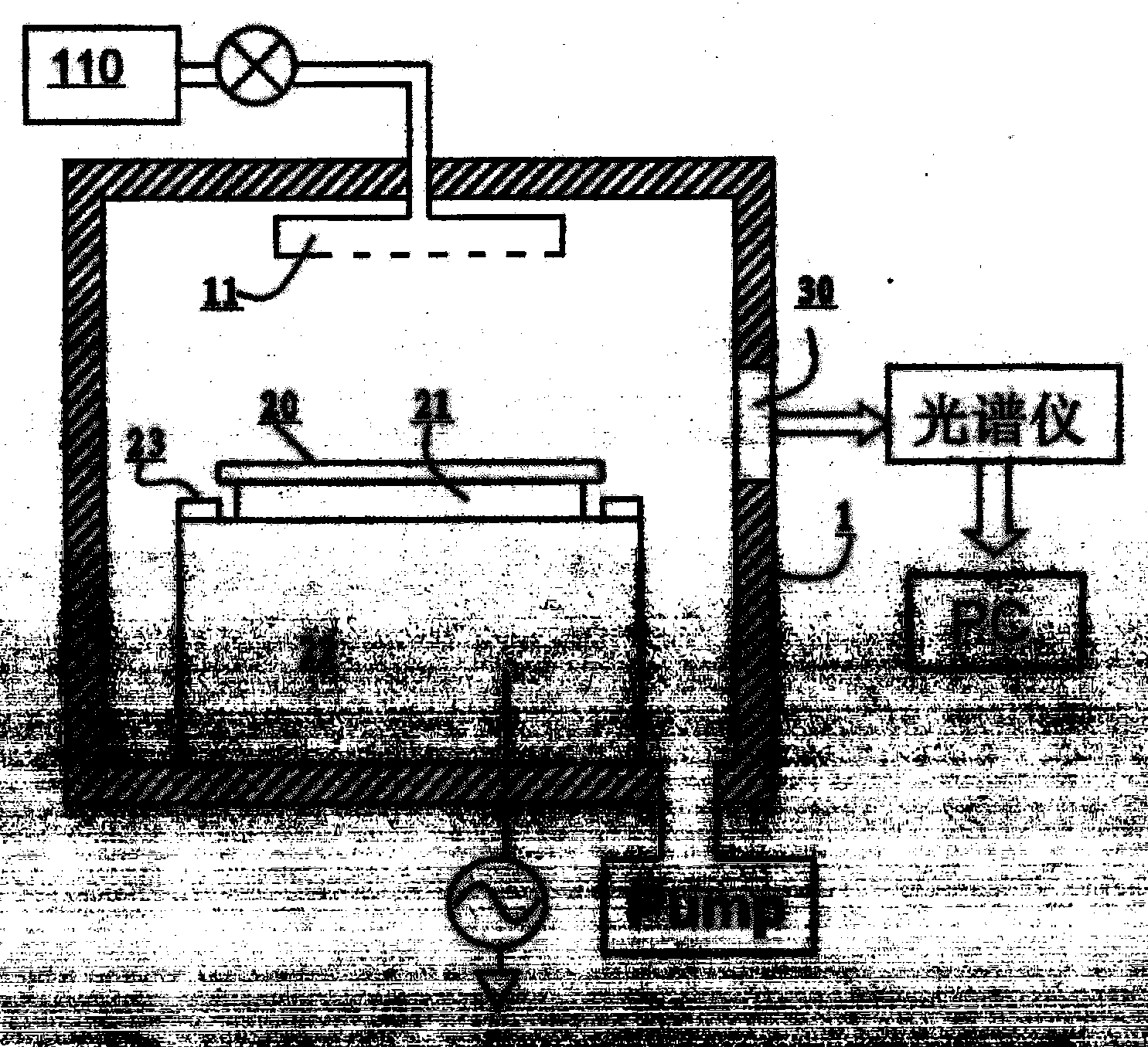
[0018] The invention provides a gas leakage detection method for a vacuum reaction chamber. The vacuum reaction chamber can be a widely used plasma etching or chemical deposition reaction chamber, or other reaction chambers that require a vacuum state. figure 1 It is a typical plasma etching reaction chamber. The reaction chamber includes an outer chamber wall 1, and a gas distribution device such as a shower head 11 on the top of the chamber. The shower head receives the reaction gas from the gas source 110 and distributes it evenly into the reaction chamber At the same time, the gas distribution device 11 also serves as the upper electrode for plasma generation. The lower part of the reaction chamber includes a pedestal 22 on which a processing substrate fixing device 21 is arranged. The substrate fixing device 21 can be an electrostatic chuck (ESC) or other mechanical fixing devices. The substrate 20 is placed on the substrate holding device 21 . An edge ring 23 is placed...