Thin-film transistor array substrate, liquid crystal display device and manufacturing method thereof

A technology for liquid crystal displays and thin film transistors, which is applied in the manufacture of semiconductor/solid-state devices, electric solid-state devices, semiconductor devices, etc., can solve the problems affecting the display effect of liquid crystal displays, the thickness of leaking plastic boxes, and the pollution of liquid crystals, so as to improve the display effect, The effect of avoiding glue leakage and avoiding pollution

Inactive Publication Date: 2012-04-11
TCL CHINA STAR OPTOELECTRONICS TECH CO LTD
View PDF3 Cites 7 Cited by
  • Summary
  • Abstract
  • Description
  • Claims
  • Application Information

AI Technical Summary

Problems solved by technology

[0006] An object of the present invention is to provide a method for manufacturing a liquid crystal display, to solve the phenomenon of glue leakage and uneven thickness of the box after bonding the TFT substrate and the CF substrate due to the uneven width and height of the sealant in the prior art. Moreover, the direct contact between the frame glue and the liquid crystal will cause the pollution of the liquid crystal, which will affect the technical problem of the display effect of the liquid crystal display.

Method used


Image

  • Thin-film transistor array substrate, liquid crystal display device and manufacturing method thereof
  • Thin-film transistor array substrate, liquid crystal display device and manufacturing method thereof
  • Thin-film transistor array substrate, liquid crystal display device and manufacturing method thereof

Examples


Embodiment Construction

[0038] The following descriptions of the various embodiments refer to the accompanying drawings to illustrate specific embodiments in which the present invention can be practiced.

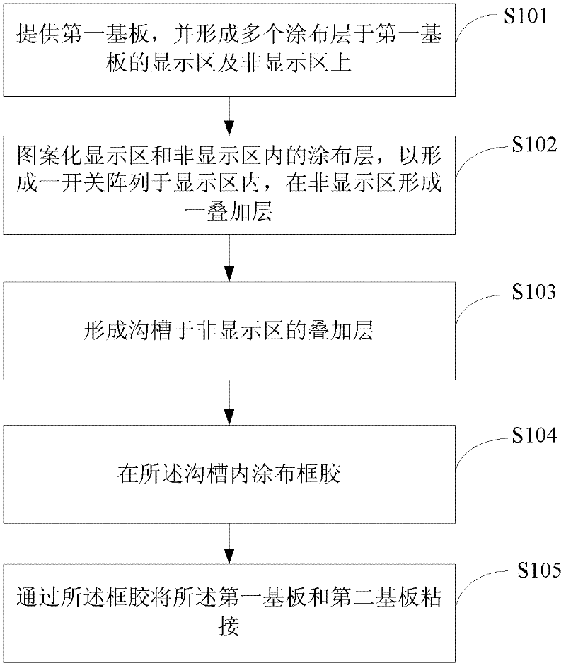
[0039] figure 1 It is a schematic flow chart of a preferred embodiment of the manufacturing method of the liquid crystal display in the present invention.

[0040] In step S101 , a first substrate is provided, and a plurality of coating layers are formed on the display area and the non-display area of ​​the first substrate.

[0041] For example, a first metal layer, a gate insulating layer, an amorphous silicon layer, an ohmic contact layer, a second metal layer, a transparent conductive layer, and a protective layer are deposited on the first substrate.

[0042] In a specific implementation process, the first substrate is a TFT substrate. Certainly, the first substrate may also be a unified body of a TFT substrate and a CF substrate.

[0043] In step S102 , the coating layer in the display area...


PUM


Abstract

The invention discloses a thin-film transistor array substrate, a liquid crystal display device and a manufacturing method thereof. The manufacturing method comprises the steps of: providing a first substrate, wherein the first substrate is provided with a display area and a non-display area, and the non-display area is located around the display area; forming a coating layer on the display area and the non-display area; respectively patterning the coating layer in the display area and the non-display area so as to form a switch array in the display area and form a superimposed layer on the non-display area, wherein the superimposed layer comprises at least one coating layer; performing exposure development to form a channel in the superimposed layer; filling frame glue in the channel; and bonding the first substrate and a second substrate by means of the frame glue. According to the invention, the shape of the frame glue can be accurately controlled, so that glue leakage can be prevented, liquid crystal can be ensured to be prevented from pollution, and box thickness is prevented from nonuniformity.

Description

【Technical field】 [0001] The invention relates to the technical field of liquid crystal production, in particular to a thin film transistor array substrate, a liquid crystal display and a manufacturing method thereof. 【Background technique】 [0002] With the continuous development of liquid crystal display technology, the requirements for the functions of liquid crystal displays are also getting higher and higher. [0003] A thin film transistor array (Thin Film Transistor, hereinafter referred to as TFT)-liquid crystal display (Liquid Crystal Display, LCD) is composed of a TFT substrate, a color filter array (Color Filter, hereinafter referred to as CF) substrate and liquid crystal between the two substrates. Among them, the TFT substrate and the CF substrate are the array substrates required for the design after film formation, exposure, development and etching by chemical or physical methods. [0004] In order to cut off the contact between the liquid crystal molecules b...

Claims


Application Information

Patent Timeline
Patent Type & Authority Applications(China)
IPC IPC(8): G02F1/1333G02F1/1339G02F1/1362G02F1/1368H01L21/77H01L27/02
CPCG02F1/1362G02F2001/133388G02F1/1339G02F1/133388
Inventor 文松贤蔡荣茂廖学士庄益壮邓明锋张小新
Owner TCL CHINA STAR OPTOELECTRONICS TECH CO LTD
Why Eureka
Try Eureka