Transmission electron microscopy sample preparation method capable of detecting Damascus seed crystal layer and barrier layer

A technology for transmission electron microscope samples and barrier layers, which is applied in the manufacture of circuits, electrical components, semiconductor/solid-state devices, etc. Layer and seed layer thickness and overlay morphology

Active Publication Date: 2012-04-11
SHANGHAI HUALI MICROELECTRONICS CORP
View PDF3 Cites 9 Cited by
  • Summary
  • Abstract
  • Description
  • Claims
  • Application Information

AI Technical Summary

Problems solved by technology

This can protect the seed layer from surface damage caused by the environment and sample preparation before TEM observation, but it is easy to cause deformation of the Damascene structure, and cannot accurately detect the thickness and coverage morphology of the barrier layer and seed layer
Another method is to directly fill the damascene structure with metal copper 03 after the deposition of the diffusion barrier l

Method used


Image

  • Transmission electron microscopy sample preparation method capable of detecting Damascus seed crystal layer and barrier layer
  • Transmission electron microscopy sample preparation method capable of detecting Damascus seed crystal layer and barrier layer
  • Transmission electron microscopy sample preparation method capable of detecting Damascus seed crystal layer and barrier layer

Examples


preparation example Construction

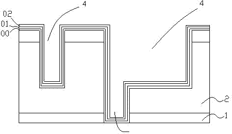
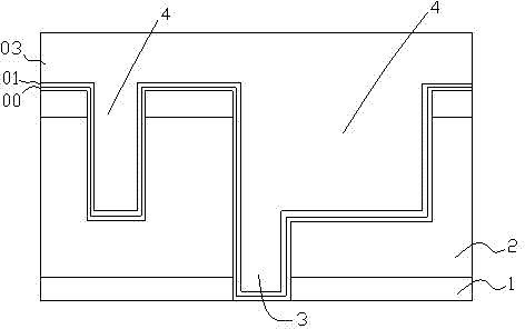
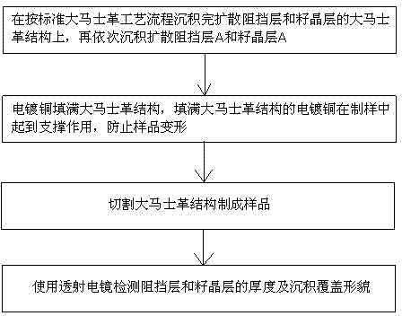
[0027] like image 3 As shown, the method for preparing a transmission electron microscope sample capable of detecting the damascene seed layer and the barrier layer of the present invention specifically includes the following steps: on the damascene structure that has deposited the diffusion barrier layer 00 and the seed layer 01 according to the standard damascene process flow, and then sequentially deposits Diffusion barrier layer A 00' and seed layer A 01'; then use metal copper 03 to fill the Damascus structure, and the metal copper 03 filled with Damascus structure plays a supporting role in sample preparation to prevent sample deformation, and metal copper 03 is filled with Damascus Specifically, electroplating process or physical vapor deposition technology can be used for the structure; then the damascus structure can be cut to make samples, specifically, the focused ion beam (FIB) cutting can be used to prepare transmission electron microscope samples or samples can b...


PUM

PropertyMeasurementUnit
Thicknessaaaaaaaaaa
Thicknessaaaaaaaaaa

Abstract

The invention discloses a transmission electron microscopy sample preparation method capable of detecting a Damascus seed crystal layer and a barrier layer, which includes the following steps: a diffusion barrier layer A and a seed crystal layer A are sequentially deposited again on a Damascus structure on which the diffusion barrier layer and the seed crystal layer are already deposited according to the standard Damascus process; copper is filled in the Damascus structure, and the copper filled in the Damascus structure plays the supporting role in sample preparation to prevent the deformation of a sample; the Damascus structure is cut into the sample; and transmission electron microscopy is used for detecting the thicknesses of the barrier layers and the seed crystal layers and the deposit coverage topography. Since the transmission electron microscopy sample preparation method utilizes the copper to fill the Damascus structure, the surface of the seed crystal layers can be prevented from being injured by the environment and sample preparation before transmission electron microscopy observation, the copper plays the supporting role in the focused ion beam cutting process, and therefore can prevent the deformation of the Damascus structure caused by sample preparation, and a TEM (transmission electron microscopy) picture can truly reflect the thicknesses of the barrier layers and the seed crystal layers and the deposit coverage topography at the same time.

Description

technical field [0001] The present invention generally relates to the field of semiconductor manufacturing copper interconnection, more precisely, the present invention relates to a transmission electron microscope sample preparation method that can simultaneously detect the thickness of the seed layer and barrier layer and the deposition coverage morphology in the damascene copper interconnection process. Background technique [0002] As the size of CMOS transistors continues to shrink to the sub-micron level, as predicted by Moore's Law, the number of transistors in high-efficiency, high-density integrated circuits rises to tens of millions. The signal integration of these huge number of active components requires more than eight layers of high-density metal wiring. However, the resistance and parasitic capacitance brought by these metal interconnections have become the main factors that limit the speed of this efficient integrated circuit. Driven by this factor, the semic...

Claims


Application Information

Patent Timeline
IPC IPC(8): H01L21/768H01L21/02
Inventor 李磊胡友存姬峰张亮陈玉文
Owner SHANGHAI HUALI MICROELECTRONICS CORP
Why Eureka
Try Eureka