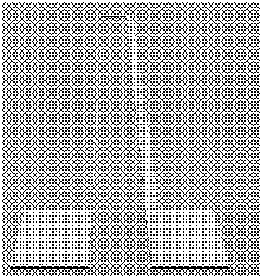
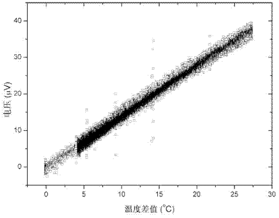
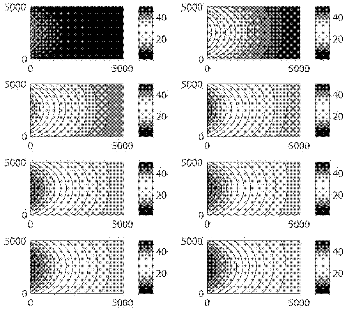
Metal film micron-scale thermocouple device
A metal thin film and thermocouple technology, applied in instruments, thermometers, measuring heat, etc., can solve the problems of the flatness of the test plane, the stability and accuracy of the thermocouple, etc., and achieve a simple and easy temperature measurement method and improve accuracy Accuracy and stability, the effect of accurate temperature measurement
- Summary
- Abstract
- Description
- Claims
- Application Information
AI Technical Summary
Problems solved by technology
Method used
Image
Examples
example 1
[0019] 1. Design and manufacture a mask plate with a single metal thin film thermocouple. The width of the two arms of the thermocouple is 1.5 microns and 200 microns respectively;
[0020] 2. Select glass as the substrate, and obtain a circular substrate with a diameter of 2 inches and a thickness of 0.6 mm through cutting and grinding processes. Clean the substrate with acetone, alcohol, and deionized water in an ultrasonic cleaner for 5 minutes to ensure the surface is clean;
[0021] 3. After the substrate is cleaned, select the 5350 photoresist (German ALLRESIST company) commonly used in the microelectronics process, and make the photoresist evenly adhere to the surface of 1 μm through a homogenizer at a speed of 4000 rpm for 1 minute. Bake for 30 minutes at celsius. After that, use the mask plate to expose through ultraviolet light, use the MJB4 lithography machine of SUSS MicroTec Company, under the power intensity of 300W mercury lamp, expose for 2.5s, and then use AR...
example 2
[0024] 1. Design and manufacture a reticle with a single metal thin film thermocouple array, the array is composed of multiple thermocouples, and the width of each thermocouple's two arms is 3 microns and 100 microns respectively;
[0025] 2. Select glass as the substrate, and obtain a circular substrate with a diameter of 2 inches and a thickness of 0.6 mm through cutting and grinding processes. Clean the substrate with acetone, alcohol, and deionized water in an ultrasonic cleaner for 5 minutes to ensure the surface is clean;
[0026] 3. After the substrate is cleaned, select the 5350 photoresist (German ALLRESIST company) commonly used in the microelectronics process, and make the photoresist evenly adhere to the surface of 1 μm through a homogenizer at a speed of 4000 rpm for 1 minute. Bake for 30 minutes at celsius. After that, use the mask plate to expose through ultraviolet light, use the MJB4 lithography machine of SUSS MicroTec Company, under the power intensity of 3...
PUM
| Property | Measurement | Unit |
|---|---|---|
| width | aaaaa | aaaaa |
| width | aaaaa | aaaaa |
Abstract
Description
Claims
Application Information
 - R&D
- Intellectual Property
- Life Sciences
- Materials
- Tech Scout
- Unparalleled Data Quality
- Higher Quality Content
- 60% Fewer Hallucinations
Browse by: Latest US Patents, China's latest patents, Technical Efficacy Thesaurus, Application Domain, Technology Topic, Popular Technical Reports.
© 2025 PatSnap. All rights reserved.Legal|Privacy policy|Modern Slavery Act Transparency Statement|Sitemap|About US| Contact US: help@patsnap.com


