Method of forming micro-pore structures or trench structures on surface of silicon wafer substrate

A substrate surface, microporous structure technology, applied in photovoltaic power generation, electrical components, circuits, etc., can solve the problem of high manufacturing cost

Inactive Publication Date: 2012-05-09
纮泰科技股份有限公司
View PDF6 Cites 22 Cited by
  • Summary
  • Abstract
  • Description
  • Claims
  • Application Information

AI Technical Summary

Problems solved by technology

However, before the chemical etching step in the above-mentioned prior art, high-priced precious metal elements (such as silver elements) must be deposited, and the manufacturing cost is relatively high.

Method used


Image

  • Method of forming micro-pore structures or trench structures on surface of silicon wafer substrate
  • Method of forming micro-pore structures or trench structures on surface of silicon wafer substrate
  • Method of forming micro-pore structures or trench structures on surface of silicon wafer substrate

Examples


Embodiment 1

[0063] A sliced, smooth-surfaced monocrystalline silicon chip (about 150 cm in size) was prepared, and the following aqueous solution was prepared.

[0064] Cleaning solution: an aqueous solution of 30% hydrogen peroxide and 98% concentrated sulfuric acid mixed at a ratio of 1:4 (volume ratio).

[0065] Electroless co-plating solution: containing 0.05mol / L silver nitrate (AgNO 3 ), 0.05mol / L zinc nitrate (Zn(NO 3 ) 2 ) and 1.0mol / L sodium hydroxide (NaOH) mixed aqueous solution.

[0066] Etching solution: an aqueous solution mixed with 10% hydrofluoric acid and 30% hydrogen peroxide at a ratio of 10:1 (volume ratio).

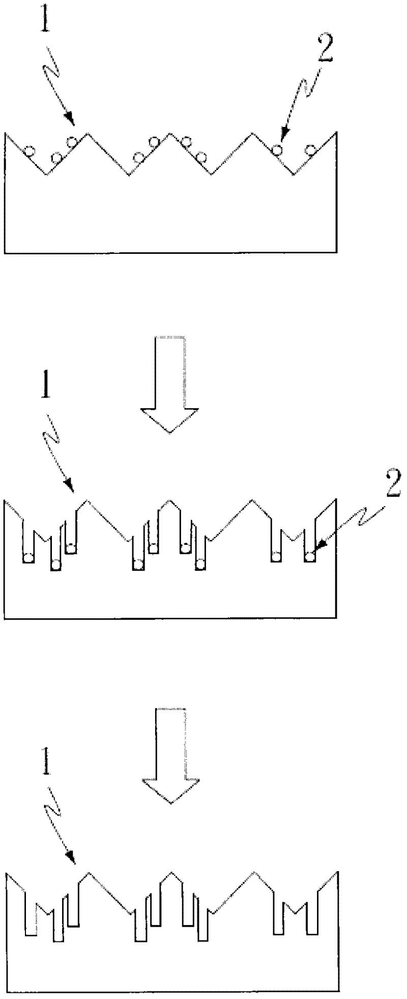
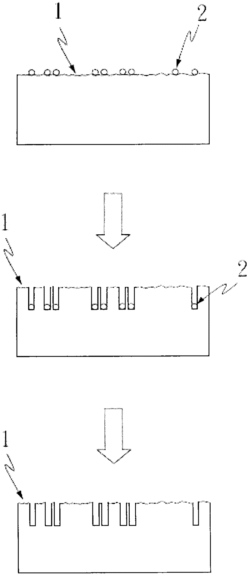
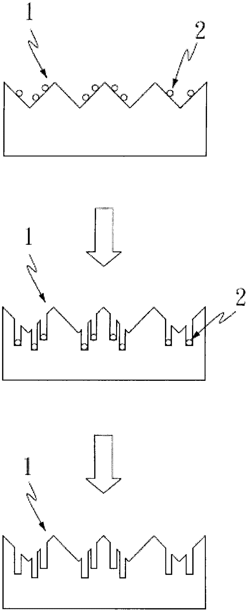
[0067]The chip was soaked in the cleaning solution for 10 minutes to clean the chip. Next, soak the chip in the electroless co-plating chemical solution for about 20 minutes, so that the alloy particles formed by silver and zinc are deposited on the surface of the chip. Second, soak the chip deposited with the silver-zinc alloy particles in the etching solu...

Embodiment 2

[0069] Except that the 0.05mol / L zinc nitrate of the electroless co-plating liquid in embodiment 1 is replaced by 0.02mol / L tin sulfate (SnSO 4 ), all the other implementation conditions and steps are the same as in Example 1.

Embodiment 3

[0071] Except that silver nitrate and zinc nitrate of the electroless co-plating liquid in embodiment 1 are replaced by silver sulfate (Ag 2 SO 4 ) and zinc sulfate (ZnSO 4 ), all the other implementation conditions and steps are the same as in Example 1.


PUM

PropertyMeasurementUnit
particle diameteraaaaaaaaaa
diameteraaaaaaaaaa
diameteraaaaaaaaaa

Abstract

A method of forming micro-pore structures or trench structures on a surface of a silicon wafer substrate comprises (A) forming at least a noble-metal alloy particle on the surface of the silicon wafer substrate; and (B) then followed by employing a chemical wet etching on the surface of the silicon wafer substrate. During the processes, noble-metal alloy particle is used to catalyze the oxidation of the silicon wafer substrate surface in contact therewith, and an etchant is used to simultaneous etch the silicon dioxide to result in local micro-etching at the surface of the silicon wafer substrate, thereby forming micro-pore structures or trench structures on the surface of the silicon wafer substrate. Surface reflectivity of the silicon chip substrate can be effectively reduced. The method increases the power conversion efficiency of the solar cells and reduces the manufacturing costs so as to increase the production benefits of the solar cells.

Description

technical field [0001] The invention relates to a method for forming a microporous structure or a groove structure on the surface of a silicon chip substrate, especially a chemical etching method for forming a microporous structure or a groove structure on the surface of a silicon chip substrate through noble metal alloy particles. Background technique [0002] In recent years, the price of international energy (especially oil) has been rising day by day, and the demand for energy has also become increasingly tense. Renewable energy is a green energy that does not harm the environment, among which solar cells are a very promising clean energy that can generate electricity directly from sunlight. A solar cell is an energy-converting photoelectric component that converts light energy into electrical energy after being irradiated by sunlight. However, at present, the production cost of solar cells must be effectively reduced before they can be widely accepted as the main sourc...

Claims


Application Information

Patent Timeline
Patent Type & Authority Applications(China)
IPC IPC(8): C23F1/02C23F1/24
CPCH01L31/0236Y02E10/547H01L31/068H01L21/30604H01L31/028H01L21/0203H01L31/02363H01L21/306
Inventor 钱家锜林育玫高伟哲江漪凌
Owner 纮泰科技股份有限公司
Why Eureka
Try Eureka