Array base plate, liquid crystal display and manufacturing method for array base plate

An array substrate and manufacturing method technology, applied in the field of liquid crystal display, can solve problems such as damage to TFT channels, achieve the effects of improving performance, improving production efficiency, and reducing the number of photolithography times

Inactive Publication Date: 2012-05-09
BOE TECH GRP CO LTD
View PDF7 Cites 19 Cited by
  • Summary
  • Abstract
  • Description
  • Claims
  • Application Information

AI Technical Summary

Problems solved by technology

[0022] The invention provides an array substrate, a liquid crystal display and a method for manufacturing the array substrate, so as to solve the problem of damaging the TFT channel in the prior art when manufacturing the array substrate, and improve the performance and production efficiency of the array substrate

Method used


Image

  • Array base plate, liquid crystal display and manufacturing method for array base plate
  • Array base plate, liquid crystal display and manufacturing method for array base plate
  • Array base plate, liquid crystal display and manufacturing method for array base plate

Examples


Embodiment 1

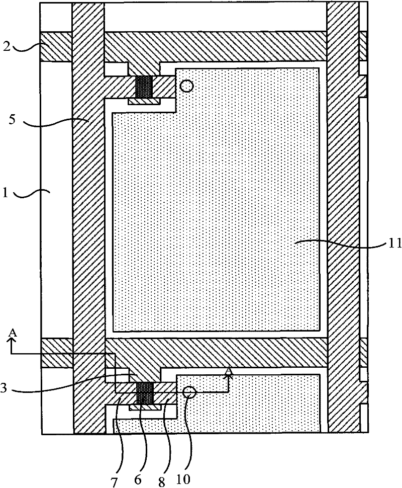
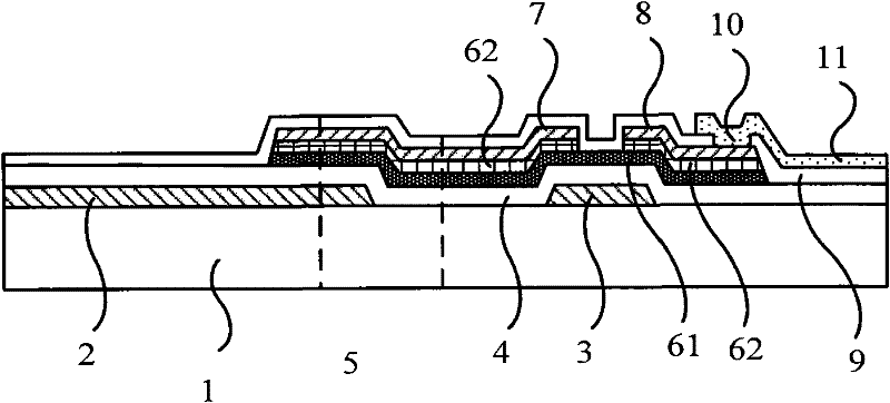
[0060] Figure 2A A partial top view structural schematic diagram of the array substrate provided by Embodiment 1 of the present invention; Figure 2B for Figure 2A Schematic diagram of the cut-away structure in side view along line A-A. Such as Figure 2A and Figure 2B As shown, the array substrate of this embodiment includes: a base substrate 1 on which gate lines 2, data lines 5, thin film transistors (TFT), pixel electrodes 11, active layer 6, and passivation layer 9 are formed. and gate insulating layer 4. Wherein, the TFT includes a gate electrode 3 , a source electrode 7 and a drain electrode 8 ; the gate electrode 3 is connected to the gate line 2 , the source electrode 7 is connected to the data line 5 , and the drain electrode 8 is connected to the pixel electrode 11 . Wherein, the gate insulating layer 4 is formed above the gate electrode 3; the active layer 6 is formed above the gate insulating layer 4; the passivation layer 9 is formed above the active laye...

Embodiment 2

[0085] Figure 6A It is a flow chart of the manufacturing method of the array substrate provided by Embodiment 2 of the present invention. Such as Figure 6A As shown, the method of the present embodiment includes:

[0086] Step 61, depositing a transparent conductive film and a gate metal film on the base substrate, and forming a pattern including a pixel electrode, a gate electrode and a gate line through a patterning process;

[0087] Step 62, depositing a gate insulating layer film, an active layer film and a passivation layer film on the base substrate forming the above pattern, and forming a pattern including a passivation layer, an active layer and a gate insulating layer through a patterning process; wherein, the passivation layer The gate insulating layer includes a source electrode via hole and a drain electrode via hole; the gate insulating layer includes a contact via hole, and the contact via hole is located above the pixel electrode;

[0088] Step 63. Deposit ...


PUM


Abstract

The invention discloses an array base plate, a liquid crystal display and a manufacturing method for the array base plate. The array base plate comprises a substrate base plate; a grid line, a data wire, a thin film transistor, a pixel electrode, an active layer, a passivation layer and a grid insulating layer are formed on the substrate base plate; the thin film transistor comprises a grid electrode connected with the grid line, a source electrode connected with the data wire and a drain electrode connected with the pixel electrode; the grid insulating layer is formed above the grid electrode; the passivation layer is arranged among the active layer, the source electrode and the drain electrode; the passivation layer is provided with a source electrode through hole and a drain electrode through hole; and the source electrode and the drain electrode are respectively connected with the active layer through the source electrode through hole and the drain electrode through hole. According to the technical scheme, the active layer, the passivation layer and the grid insulating layer are formed by one-time composition, so that the composition number is reduced and the production efficiency is improved; and meanwhile, the array base plate structure in which the passivation layer is positioned above the active layer is realized, and damage to a thin film transistor (TFT) channel when the source electrode and the drain electrode are formed is avoided.

Description

technical field [0001] The invention relates to liquid crystal display technology, in particular to an array substrate, a liquid crystal display and a manufacturing method of the array substrate. Background technique [0002] Liquid crystal display is a commonly used flat-panel display at present, among which thin film transistor liquid crystal display (ThinFilm Transistor Liquid Crystal Display; referred to as: TFT-LCD) has become the mainstream product in liquid crystal display due to its advantages of small size, low power consumption, and no radiation. . Usually TFT-LCD includes liquid crystal panel, drive circuit and backlight source. The liquid crystal panel is the main part of the TFT-LCD. It is composed of an array substrate and a color film substrate, and a liquid crystal layer is filled in between. By controlling the voltage provided by the drive circuit, the liquid crystal molecules are deflected in an orderly manner, resulting in light and dark changes of light....

Claims


Application Information

Patent Timeline
Patent Type & Authority Applications(China)
IPC IPC(8): H01L27/12H01L21/77G02F1/1362G02F1/1333
CPCH01L27/1288
Inventor 刘翔薛建设
Owner BOE TECH GRP CO LTD
Why Eureka
Try Eureka