VDMOS (Vertical Double-diffused Metal Oxide Semiconductor) transistor

A transistor and semiconductor technology, applied in the direction of semiconductor devices, electrical components, circuits, etc., can solve the problems of mutual integration of MOS transistors, increase switching loss, device current, voltage performance degradation, etc., to shorten the charge and discharge time, reduce Gate-drain capacitance, effect of increasing switching speed

Inactive Publication Date: 2012-05-16
GRACE SEMICON MFG CORP
View PDF4 Cites 14 Cited by
  • Summary
  • Abstract
  • Description
  • Claims
  • Application Information

AI Technical Summary

Problems solved by technology

[0006] In the prior art, there are generally two ways to reduce the gate-drain capacitance Cgd of a MOS transistor: one way is to reduce the area of ​​the gate and the drain, but this method will bring a larger on-resistance Rds(on ), while increasing the switching loss, it will also cause a decrease in device current, voltage and other performance; another method is to reduce the relative contact area between the gate and the drain, usually using a certain method for the gate Shielding technology, thereby reducing the relative capacitance of the gate-drain, in the Chinese patent CN03817927.X, a semiconductor gate structure including a shielding electrode and a switch electrode is provided, although this structure reduces the gate-drain to a certain extent. Relative capacitance, but the structure involves more process steps, and the preparation method is more complicated, which increases the manufacturing cost of the MOS transistor. In addition, the structure involves multiple dielectric layers, and its dimensional accuracy is not easy to control, which affects other properties of the MOS transistor and MOS The mutual integration between devices has a certain influence

Method used


Image

  • VDMOS (Vertical Double-diffused Metal Oxide Semiconductor) transistor
  • VDMOS (Vertical Double-diffused Metal Oxide Semiconductor) transistor
  • VDMOS (Vertical Double-diffused Metal Oxide Semiconductor) transistor

Examples


Embodiment Construction

[0022] In order to make the object, technical solution and advantages of the present invention clearer, the present invention will be further described in detail below in conjunction with the accompanying drawings.

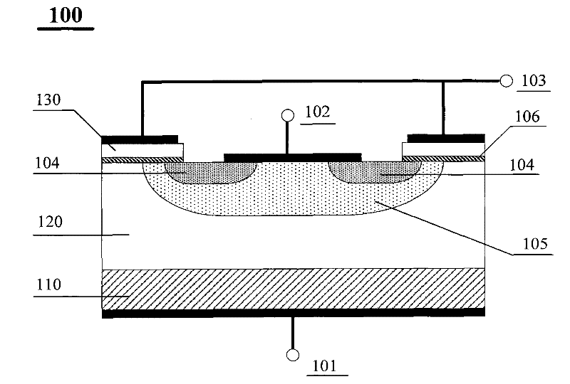
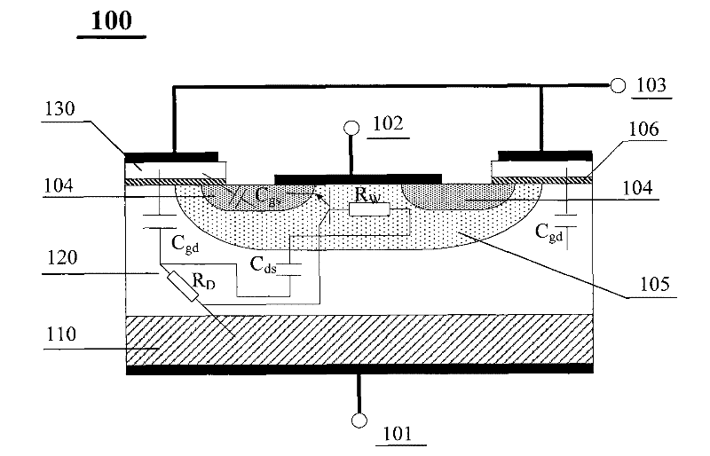
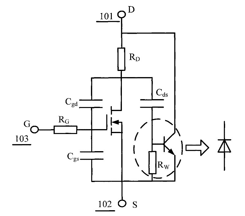
[0023] figure 2 It is a schematic diagram of the first embodiment of the VDMOS transistor provided by the present invention.

[0024] Such as figure 2 As shown, VDMOS transistor 200 includes:

[0025] a semiconductor substrate 210 of the first conductivity type;

[0026] An epitaxial layer 220 of the first conductivity type covering the surface of the semiconductor substrate 210;

[0027] A source doped region 201 of the first conductivity type and a channel region 202 of the second conductivity type located in the epitaxial layer 220;

[0028] A gate oxide layer 203 covering the surface of the epitaxial layer 220 and other parts except the source doped region 201;

[0029] An insulating dielectric layer 205 located on the upper surface of the gate oxide la...


PUM


Abstract

The invention relates to a VDMOS (Vertical Double-diffused Metal Oxide Semiconductor) transistor, belonging to the field of semiconductor devices. The VDMOS transistor comprises a semiconductor substrate, an epitaxial layer, a source doping region, a channel region, a gate oxide layer and a polysilicon gate, and an insulation dielectric layer with a thickness larger than that of the gate oxide layer is deposited at the side of the channel region between the polysilicon gate and the gate oxide layer in a horizontal direction through PECVD (Plasma Enhanced Chemical Vapor Deposition) process. By introducing the insulation dielectric layer, the relative distance between the polysilicon gate and the epitaxial layer is increased, namely the distance between the two polar plates of the gate-drain capacitance of the device is increased, thus under the condition that the area of the polysilicon gate is not changed and the on-resistance of the device is not increased, the gate-drain capacitance of the device is effectively reduced; the charging and discharging time for the gate-drain capacitance during the switching of the MOS (Metal Oxide Semiconductor) transistor is greatly reduced, the switching speed of the MOS transistor is increased, the dynamic loss is reduced, and therefore the performance of the device is greatly improved.

Description

technical field [0001] The invention relates to a MOS transistor structure, in particular to a VDMOS transistor structure, and belongs to the field of semiconductor devices. Background technique [0002] In semiconductor integrated circuits, the circuit based on double-diffused MOS transistors, referred to as DMOS, uses the difference in lateral diffusion speed of two impurity atoms to form a self-aligned sub-micron channel, which can achieve high operating frequency and speed. The DMOS transistors can be divided into two types: lateral DMOS transistors (LDMOS for short) and vertical DMOS transistors (VDMOS). Among them, vertical DMOS transistors are increasingly used in the field of semiconductor integrated circuits due to their good performance and high integration. [0003] Figure 1a It is a schematic cross-sectional structure diagram of a traditional VDMOS transistor 100 . Such as Figure 1a As shown, the vertical double diffused MOS transistor 100 at N + A layer of...

Claims


Application Information

Patent Timeline
Patent Type & Authority Applications(China)
IPC IPC(8): H01L29/78H01L29/06
Inventor 王颢
Owner GRACE SEMICON MFG CORP
Why Eureka
Try Eureka