Wet chemical cleaning method

A wet chemistry, oxide layer technology, applied in electrical components, semiconductor/solid-state device manufacturing, circuits, etc., can solve problems such as increasing process cost and increasing process time, increasing process cost, shortening process time, and eliminating the formation of water. trace effect

Inactive Publication Date: 2012-05-23
CSMC TECH FAB1 +1
View PDF4 Cites 2 Cited by
  • Summary
  • Abstract
  • Description
  • Claims
  • Application Information

AI Technical Summary

Problems solved by technology

[0004] Although the above method has reduced the possibility of forming water marks on the surface of the semiconductor wafer to a certain extent, in the process of implementing the above process, one or more cationic surfactants need to be added, and then an organic solvent must be added to c

Method used


Image

  • Wet chemical cleaning method
  • Wet chemical cleaning method
  • Wet chemical cleaning method

Examples


Embodiment 1

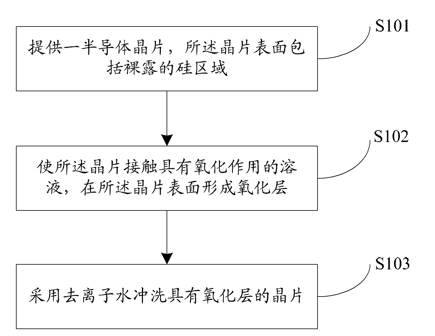
[0033] Based on the above reasons, the flow chart of the wet chemical cleaning method provided in this embodiment is as follows figure 1 As shown, the method includes the following steps:

[0034] Step S101: providing a semiconductor wafer, the surface of the wafer includes a bare silicon region;

[0035] The semiconductor wafer described in this embodiment may include semiconductor elements, such as silicon or silicon germanium (SiGe) with a single crystal, polycrystalline or amorphous structure, or a mixed semiconductor structure, such as silicon carbide; it may also be epitaxial silicon on insulator (silicon on insulator, SOI). Furthermore, the semiconductor wafer can also comprise other materials, such as multilayer structures of epitaxial layers or buried layers. In addition, the above-mentioned semiconductor wafer also includes a plurality of integrated circuits fabricated thereon, and these integrated circuits may be at any stage in the process. Therefore, the above-m...

Embodiment 2

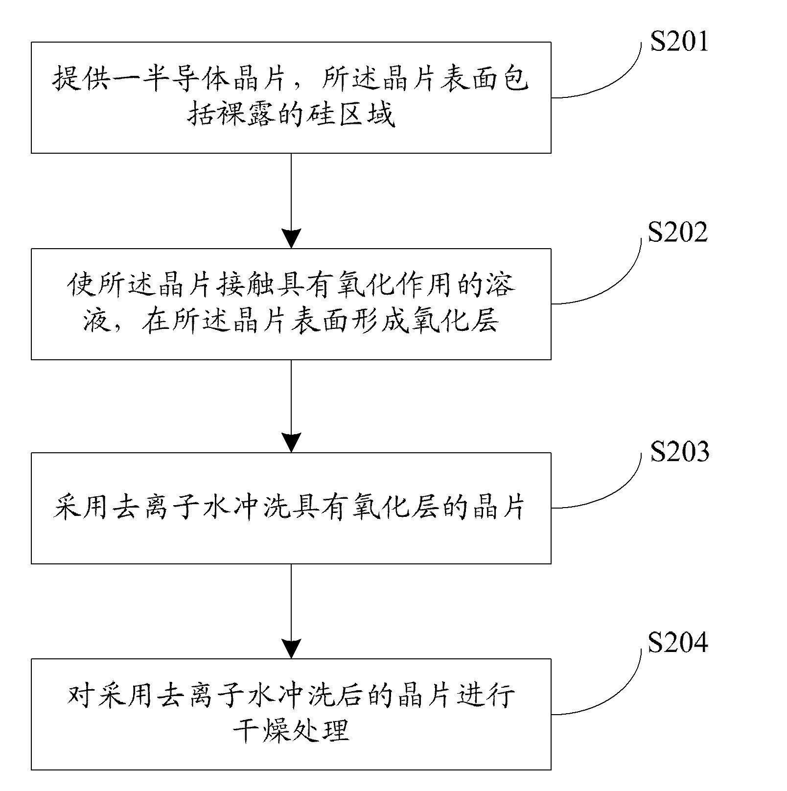
[0045] The flow chart of the wet chemical cleaning method provided in this embodiment is as follows figure 2 As shown, step S204 is added compared to Embodiment 1: dry the wafer after rinsing with deionized water, which can be dried by rotary drying, or by isopropanol vapor, or by other methods. For drying treatment, spin-drying is preferred in this embodiment, but which method should be used for drying should be comprehensively determined by the size and surface characteristics of the wafer and subsequent processes.

[0046] The oxidation solution in this example includes H 2 o 2 and H 2 O, and H 2 o 2 and H 2 O is mixed in a volume ratio of 1:5-50, preferably H 2 o 2 and H 2 O is mixed in a volume ratio of 1:10-40, more preferably H 2 o 2 and H 2 O is mixed in a volume ratio of 1: 20-30, and the concentration of the solution can be selected to match the contact time and the contact mode between the wafer and the solution with oxidation, as long as the semiconduct...

Embodiment 3

[0049] The difference between the wet chemical cleaning method provided in this example and the previous example is the selection of the solution with oxidation function. The solution with oxidation function in this example includes NH 4 OH, H 2 o 2 and H 2 O, where NH 4 OH, H 2 o 2 and H 2 O is mixed in a volume ratio of 1:1-2:5-80, preferably NH 4 OH, H 2 o 2 and H 2 O is mixed by volume ratio 1: 1-2: 5-7, promptly selects the No. 1 standard cleaning solution (SC-1) in the RCA cleaning for use, because what selected is the solution commonly used in the existing production process, so compared with the prior art The process cost is reduced.


PUM


Abstract

The embodiment of the invention discloses a wet chemical cleaning method. The wet chemical cleaning method comprises the following steps of: providing a semiconductor wafer, wherein the surface of the wafer comprises an exposed silicon region; contacting the wafer with a solution with an oxidation effect and forming an oxidation layer on the surface of the wafer; and washing the wafer with the oxidation layer by using deionzied water. By the method, one thin oxidation layer is formed on the surface of the semiconductor wafer and silicon exposed on the surface of the wafer is prevented from being directly contacted with the deionized water, so that when the wafer is washed by using the deionized water, no exposed silicon is dissolved into water, the silicon is not separated out in the subsequent drying process and the possibility of forming water track on the surface of the semiconductor wafer is reduced. According to the method, the solution with the oxidation effect in the conventional production process can be adopted, so the process cost is reduced.

Description

technical field [0001] The invention relates to the technical field of semiconductor manufacturing, more specifically, to a wet chemical cleaning method. Background technique [0002] In the manufacturing process of semiconductor wafers, it is necessary to avoid the occurrence of wafer surface defects as much as possible. The water marks produced on the wafer surface during the traditional chemical treatment process are a kind of surface defects. Usually, after a semiconductor wafer covered with a layer of oxide is subjected to wet chemical treatment, such as dipping with a diluted hydrofluoric acid solution, there will be exposed silicon areas on the surface of the semiconductor wafer, and then rinsed with deionized water. Semiconductor wafers to remove the chemical liquid remaining on the surface of the wafer after the previous chemical treatment. However, the exposed silicon on the wafer surface can dissolve when in contact with deionized water and form the reaction prod...

Claims


Application Information

Patent Timeline
IPC IPC(8): H01L21/02
Inventor 王宇澄叶鹏
Owner CSMC TECH FAB1
Why Eureka
Try Eureka