Low-roughness silicon wafer alkali corrosion process

A low-roughness, alkali-etching technology, applied in the field of low-roughness silicon wafer alkali-etching process, can solve problems such as the adverse effects of subsequent polishing and poor surface roughness of alkali-corrosion wafers, meet the requirements, speed up the corrosion rate, and improve the The effect of surface quality

Active Publication Date: 2013-06-19
ZHONGHUAN ADVANCED SEMICON MATERIALS CO LTD +1
View PDF3 Cites 0 Cited by
  • Summary
  • Abstract
  • Description
  • Claims
  • Application Information

AI Technical Summary

Problems solved by technology

[0004] Unfortunately, the roughness of the surface of the alkali corrosion sheet is usually poor, which may have an adverse effect on the subsequent polishing

Method used


Image

  • Low-roughness silicon wafer alkali corrosion process

Examples


Embodiment 1

[0018] Embodiment 1: The following is a detailed description of the alkali corrosion process of a 5-inch 375 μm thick zone-melted silicon double-sided ground silicon wafer:

[0019] 1) Select a 5-inch P-doped zone-melted silicon abrasive sheet with a thickness of 375 μm as the object of implementation, with a resistivity of 10-30Ω·cm.

[0020] 2) Use solid KOH (analytical pure) and deionized water to prepare a 47.3% KOH aqueous solution in a high-pressure water bath.

[0021] 3) Set the preparation temperature to 120°C, turn on the heater switch, and raise the temperature to the preparation temperature.

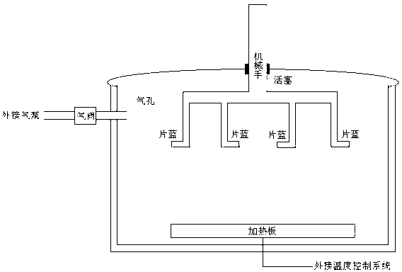
[0022] 4) Load the slices with abrasive slices into the manipulator of the high-pressure water bath, load 2 baskets of 50 slices at a time, and close the upper cover of the high-pressure water bath.

[0023] 5) Pressurize to 240Kpa; heat up to 153°C.

[0024] 6) The sinking manipulator dips the ingot into the corrosive solution, performs alkali corrosion for 3 minutes and 2...

Embodiment 2

[0039] Embodiment 2: The following is a detailed description of the alkali corrosion process of a 4-inch 410 μm thick zone-melted silicon double-sided ground silicon wafer:

[0040] 1) Select a 4-inch P-doped zone-fused silicon abrasive sheet with a thickness of 410 μm as the object of implementation, with a resistivity of 5-10Ω·cm.

[0041] 2) Use solid NaOH (analytical pure) and deionized water to prepare a 49.5% KOH aqueous solution in a high-pressure water bath.

[0042] 3) Set the preparation temperature to 120°C, turn on the heater switch, and raise the temperature to the preparation temperature.

[0043] 4) Load the flakes with abrasive flakes into the manipulator of the high-pressure water bath, load 2 baskets of 50 flakes at a time, and close the upper cover of the water bath.

[0044] 5) Pressurize to 250Kpa; heat up to 157°C.

[0045] 6) The sinking manipulator dips the ingot into the corrosive solution, carries out alkali corrosion for 2 minutes and 54 seconds, a...


PUM


Abstract

The invention relates to a low-roughness silicon wafer alkali corrosion process, which includes steps of (A) preparing alkali corrosive liquid in a high-pressure bathing kettle and setting the preparing temperature ranging from 115 DEG C to 130 DEG C; (B) immersing baskets containing grinding pieces into the alkali corrosive liquid, closing the upper cover of the high-pressure bathing kettle, pressurizing to 180Kpa to 260Kpa, heating until the temperature ranges from 145 DEG C to 160 DEG C; (C) lifting a manipulator after 1-to-10-minute alkali corrosion; (D) opening an air valve for discharging air until the pressure reaches the value of the standard atmospheric pressure, opening the upper cover of the high-pressure bathing kettle, taking off the baskets to be immersed in diluted hydrochloric acid solution, and quickly discharging, washing, drying and testing after immersion; (E) compensating water into the high-pressure bathing kettle by the aid of a hot water tank, keeping concentration proportion of corrosive liquid, and heating the water to the preparing temperature. By adjusting original process of alkali corrosion, the alkali corrosion system has the capability of producing silicon wafer with roughness lower than 1 mu m, better surface quality is provided for the next procedure of polishing, and accordingly, requirements of markets for substrate materials of devices are met.

Description

technical field [0001] The invention relates to a method for producing single crystal silicon wafers, in particular to an alkali etching process for silicon wafers with low roughness. Background technique [0002] With the continuous advancement of the technology of power electronic devices, especially the wide application of energy-saving power devices, the rapid development of silicon wafer polishing wafers as the base material for power devices has been driven. The production process of silicon wafers starts from silicon single crystal ingots, and generally includes slicing, chamfering, grinding, etching, back treatment, polishing, cleaning, and finally a polished piece with a perfect mirror surface. There are high requirements on the surface morphology of the chip and the granularity of the environment. This is because the perfect mirror surface cannot be achieved by polishing. The damaged layer on the surface of the silicon wafer after grinding is thick and needs to be...

Claims


Application Information

Patent Timeline
Patent Type & Authority Patents(China)
IPC IPC(8): C23F1/40
Inventor 罗翀张俊生李满严政先
Owner ZHONGHUAN ADVANCED SEMICON MATERIALS CO LTD
Why Eureka
Try Eureka