Multifunctional test circuit of integrated circuit stress degradation and test method thereof

A multi-functional testing, integrated circuit technology, applied in the direction of electronic circuit testing, etc.

Active Publication Date: 2014-06-11
FUDAN UNIV
View PDF3 Cites 0 Cited by
  • Summary
  • Abstract
  • Description
  • Claims
  • Application Information

AI Technical Summary

Problems solved by technology

The stress degradation of the device can only be reflected by static characteristics such as IdVg and Icp, and cannot be reflected by the dynamic characteristics of the device such as delay, so it cannot be directly related to the application of the circuit

Method used


Image

  • Multifunctional test circuit of integrated circuit stress degradation and test method thereof
  • Multifunctional test circuit of integrated circuit stress degradation and test method thereof
  • Multifunctional test circuit of integrated circuit stress degradation and test method thereof

Examples


Embodiment Construction

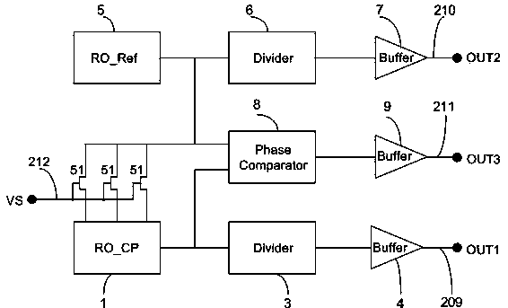
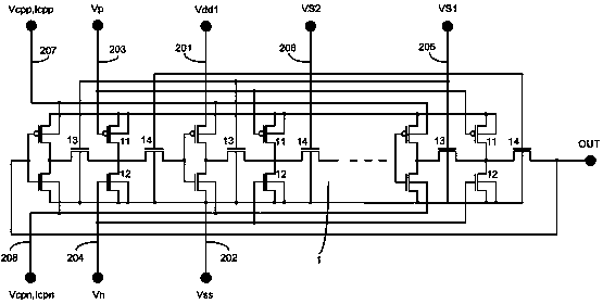
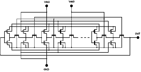
[0033] The circuit and method of the invention are used for reliability testing of integrated circuits, especially for degradation testing of CMOSFETs in integrated circuits under NBTI, PBTI, HCI and dynamic stress. The test parameters include the frequency change caused by the stress degradation of CMOSFETs in the ring oscillator inverter, and also include the CP current generated by the CMOSFETs under stress. The overall circuit as figure 1 As shown, there are a total of 15 external contact pads (Pad), which are the high power supply terminal Vdd1 of the core circuit, the low power supply terminal Vss of the core circuit, and the high power supply terminal commonly used by the reference circuit, frequency divider, buffer and phase comparator. Vdd2, the low power terminal GND commonly used by the reference circuit, frequency divider, buffer and phase comparator, the control terminal Vdd3 of all switches in the reference circuit, the control terminals VS, VS1, VS2 of the switc...


PUM


Abstract

The invention belongs to a integrated circuit reliability test technology field and especially relates to a multifunctional test circuit of integrated circuit stress degradation and a test method thereof. A core part of the test circuit takes an annular oscillator as a basis. Several auxiliary transistors, switch transistors and control terminals are added. By using the circuit and the method of the invention, a negative bias temperature instability, a positive bias temperature instability, hot hole injection or hot electron injection stress can be applied to pMOSFETs or nMOSFETs in a ring vibration inverter respectively; a ring oscillator is in a normal oscillation and stress oscillation state; the pMOSFETs or nMOSFETs of the inverter in the ring oscillator is in a measuring state of a charge pump. The degradation of the MOSFETs in the ring vibration inverter can be shown through changes of a ring oscillator oscillation frequency after the stress and can be shown through the changes of a CP current (Icpp or Icpn) of the pMOSFETs or nMOSFETs in the ring oscillator.

Description

technical field [0001] The invention belongs to the technical field of reliability testing of integrated circuits, and in particular relates to a testing circuit and a testing method for stress degradation of integrated circuits. Background technique [0002] Bias temperature instability (BTI) and hot carrier injection (HCI) are two fundamental issues affecting the reliability of complementary metal-oxide-semiconductor field-effect transistors (CMOSFETs). For nanoscale CMOSFETs composed of SiO2 or SiON gate dielectrics, the negative bias temperature instability (NBTI) of pMOSFETs is the main reason affecting the device lifetime. However, for CMOSFETs constructed of high-k gate dielectrics, both the positive bias temperature instability (PBTI) of nMOSFETs and the HCI of p and nMOSFETs have a significant impact on device reliability. [0003] BTI and HCI degradation result in reduced drive current for MOSFETs, or increased device delay. At the level of CMOS circuits, the afo...

Claims


Application Information

Patent Timeline
Patent Type & Authority Patents(China)
IPC IPC(8): G01R31/28
Inventor 黄大鸣彭嘉李名复
Owner FUDAN UNIV
Why Eureka
Try Eureka