High-isolation integrated circuit packaged by adopting ceramic casing

A high isolation, ceramic shell technology, used in circuits, electrical components, electrical solid devices, etc., can solve problems affecting the working characteristics of RF chips, malfunction of surrounding circuits and systems, and great impact on circuit performance, and achieve good applications. Prospects, reducing the number of shots, improving work efficiency and economic benefits

Active Publication Date: 2012-06-13
CHONGQING SOUTHWEST INTEGRATED CIRCUIT DESIGN +1
View PDF6 Cites 11 Cited by
  • Summary
  • Abstract
  • Description
  • Claims
  • Application Information

AI Technical Summary

Problems solved by technology

[0002] In the design of RF IC, the electromagnetic field distribution of the RF signal increases with the increase of the frequency, and its spatial distribution characteristics also increase. It affects the working characteristics of the RF chip itself, and the coupled high-frequency signal energy will also cause the surrounding circuits and systems to malfunction, resulting in serious electromagnetic interference problems
[0003] The traditional ceramic shell generally has three layers, the first dielectric layer, the metal base layer and the second dielectric layer, and the metal base layer for transmitting electrical signals is between the two dielectric layers. There is no barrier layer between the signal layers that can effectively isolate the leakage of the local oscillator, resulting in a high coupling effect between channels during the transmission of high-frequency signals, which will increase the leakage of the local oscillator of the signal, and the isolation is low

Method used


Image

  • High-isolation integrated circuit packaged by adopting ceramic casing
  • High-isolation integrated circuit packaged by adopting ceramic casing
  • High-isolation integrated circuit packaged by adopting ceramic casing

Examples


Embodiment 1

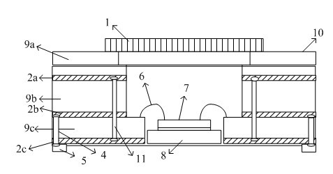
[0022] Embodiment one, see figure 1 , an integrated circuit with high isolation packaged in a ceramic case, including a tube case and a chip 7, the tube case is composed of a case bottom 8, a case 10 and a cover plate 1, the chip 7 is placed on the case bottom 8, and the case 10 includes a first dielectric layer 9a, a first metal base layer 2a, a second dielectric layer 9b, a second metal base layer 2b, a third dielectric layer 9c and a third metal base layer 2c; the first dielectric layer 9a, the first metal base layer 2a, the second dielectric layer 9b, the second metal base layer 2b, the third dielectric layer 9c and the third metal base layer 2c are laminated in order from top to bottom, and the chip 7 is connected to the second metal base layer 2a through the bonding wire 6, the second The second metal base layer 2a is connected to the lead wire 5 through the second through hole 4; the first metal base layer 2a and the third metal base layer 2c are connected through the f...

Embodiment 2

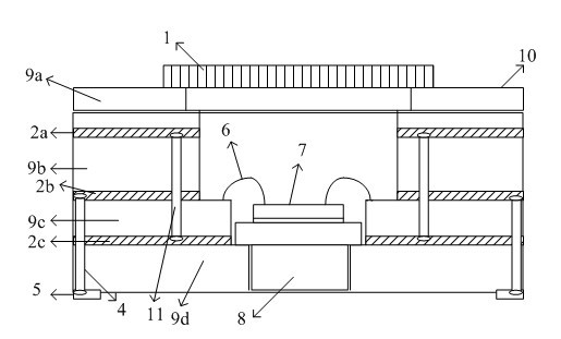
[0023] Embodiment two: see figure 2 The difference between the second embodiment and the first embodiment is that: the housing 10 also includes a fourth dielectric layer 9d, and the fourth dielectric layer 9d is laminated under the third metal base layer 2c; the shell bottom 8 is a heat sink, and the heat sink Made of tungsten-copper alloy material, the metal base layer is made of iron-nickel-cobalt alloy material, the dielectric layer is made of aluminum oxide material, and the third metal base layer 2c is connected to the shell bottom 8; when the chip does not need to dissipate heat through a heat sink, The shell bottom 8 can also be made of aluminum oxide, and connects the first metal base layer 2a to the ground.

Embodiment 3

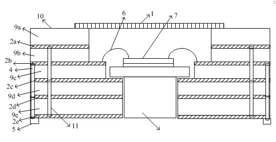
[0024] Embodiment three: see image 3 , an integrated circuit with high isolation packaged in a ceramic case, including a tube case and a chip 7, the tube case is composed of a case bottom 8, a case 10 and a cover plate 1, the chip 7 is placed on the case bottom 8, and the case 10 includes a first dielectric layer 9a, a first metal base layer 2a, a second dielectric layer 9b, a second metal base layer 2b, a third dielectric layer 9c, a third metal base layer 2c, a fourth dielectric layer 9d, a fourth metal base layer 2d, The fifth dielectric layer 9e, the fifth metal base layer 2e and the sixth dielectric layer 9f; the first dielectric layer 9a, the first metal base layer 2a, the second dielectric layer 9b, the second metal base layer 2b, the third dielectric layer 9c, The third metal base layer 2c, the fourth dielectric layer 9d, the fourth metal base layer 2d, the fifth dielectric layer 9e and the fifth metal base layer 2e are laminated in order from top to bottom, and the c...


PUM


Abstract

The invention provides a high-isolation integrated circuit packaged by adopting a ceramic casing. The integrated circuit comprises a tube shell and a chip, wherein the tube shell comprises a shell bottom, a shell and a cover plate; and the chip is arranged on the shell bottom. The integrated circuit is characterized in that the shell comprises a first dielectric layer, a first metal base layer, asecond dielectric layer, a second metal base layer, a third dielectric layer and a third metal base layer which are sequentially overlapped from top to bottom; the chip is connected with the second metal base layer through a bonding wire; and the first metal base layer is connected with the third metal base layer through a first through hole. According to the integrated circuit provided by the invention, the coupling effect of a signal channel can be effectively reduced; the leakage of a local oscillator is reduced; the chip feeding frequency can be reduced; and work efficiency and economic benefit are increased; and the integrated circuit has the advantages of high isolation, simple system structure and favorable application prospect.

Description

technical field [0001] The invention relates to an integrated circuit, in particular to an integrated circuit with high isolation and packaged in a ceramic shell. Background technique [0002] In the design of RF IC, the electromagnetic field distribution of the RF signal increases with the increase of the frequency, and its spatial distribution characteristics also increase. It affects the working characteristics of the RF chip itself, and the coupled high-frequency signal energy will also cause the surrounding circuits and systems to malfunction, resulting in serious electromagnetic interference problems. [0003] The traditional ceramic shell generally has three layers, the first dielectric layer, the metal base layer and the second dielectric layer, and the metal base layer for transmitting electrical signals is between the two dielectric layers. There is no barrier layer between the signal layers that can effectively isolate the leakage of the local oscillator, resulti...

Claims


Application Information

Patent Timeline
Patent Type & Authority Applications(China)
IPC IPC(8): H01L23/552H01L23/64
CPCH01L2224/32245H01L2224/73265H01L2924/16195H01L2224/48227H01L2224/32225H01L2924/3025H01L24/73H01L2924/14H01L2924/00H01L2924/00012
Inventor 杨若飞万天才范麟唐睿徐骅刘永光李家祎李明剑陈昆
Owner CHONGQING SOUTHWEST INTEGRATED CIRCUIT DESIGN
Why Eureka
Try Eureka