Method for packaging wafer level solid-state image sensor

A technology of solid-state image and packaging method, which is applied in the fields of decorative arts, gaseous chemical plating, microstructure devices, etc., and can solve the problem that the flatness of glass wafers and silicon wafers of image sensors is difficult to control, and the flatness of glass wafers and silicon wafers Difficult to control inter-chip spacing, by-product contamination of the chip surface, etc., to achieve an excellent planar optical window, which is beneficial to performance and avoids the distortion of image signals

Inactive Publication Date: 2012-06-20
SOUTHEAST UNIV
View PDF4 Cites 5 Cited by
  • Summary
  • Abstract
  • Description
  • Claims
  • Application Information

AI Technical Summary

Problems solved by technology

At present, people usually use thermosetting resin to bond the glass wafer and the silicon wafer to control the distance between the glass wafer and the image sensor chip. Since the thermosetting resin is filled with particles, when making through holes, the particles are easy to contaminate the chip. surface; in addition, when plasma is used to process resin, it is easy to produce by-products to contaminate the surface of the chip, resulting in a significant drop in yield to about 90%; at the same time, it is difficult to control the distance between the glass wafer and the silicon wafer
In addition, it is difficult to control the flatness of the glass wafer and silicon wafer of the image sensor packaged by this method. The patent applicant has developed several preparation methods of wafer-level glass microsphere cavity: positive pressure thermoforming and negative pressure thermoforming method

Method used


Image

  • Method for packaging wafer level solid-state image sensor
  • Method for packaging wafer level solid-state image sensor
  • Method for packaging wafer level solid-state image sensor

Examples


Embodiment 1

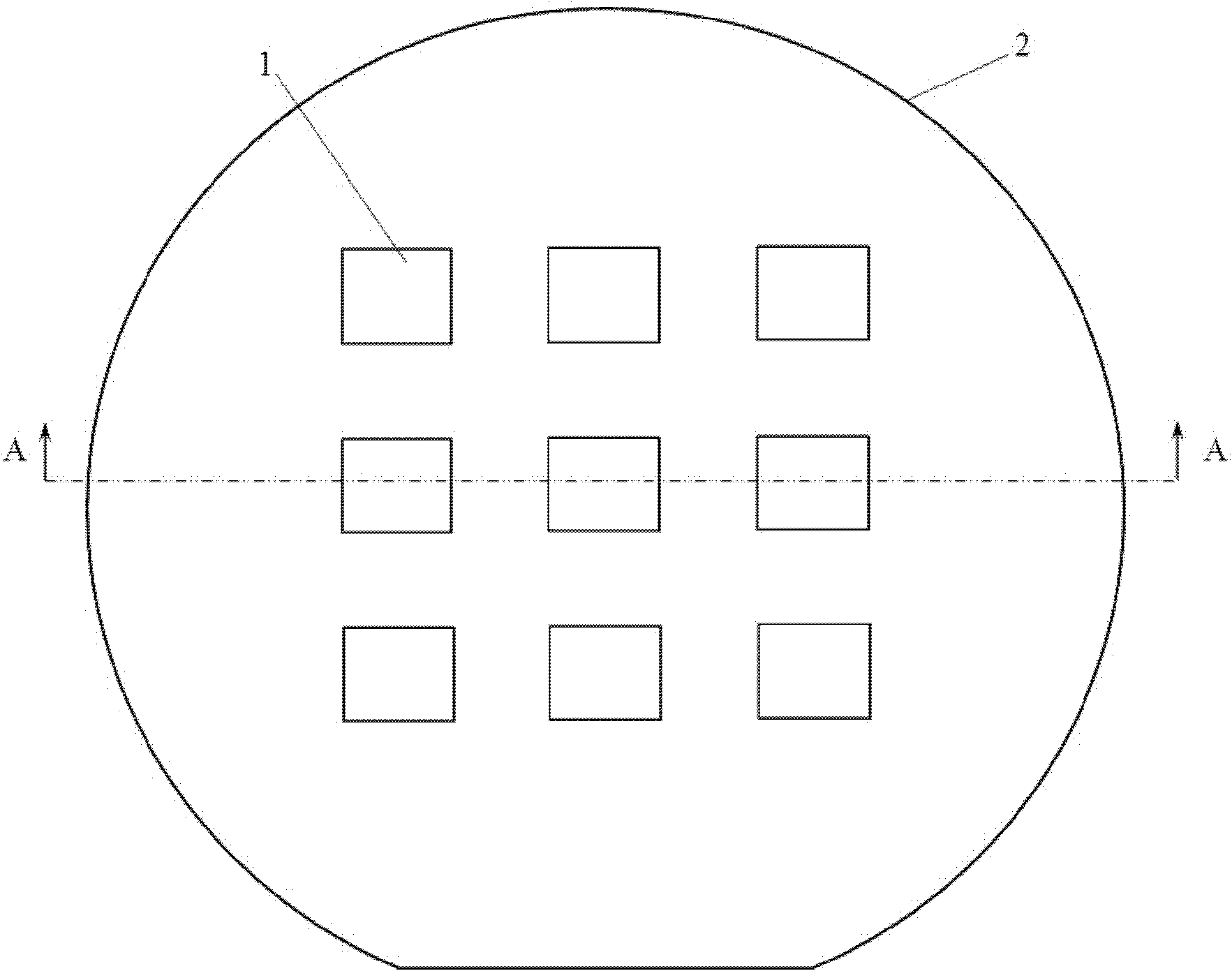
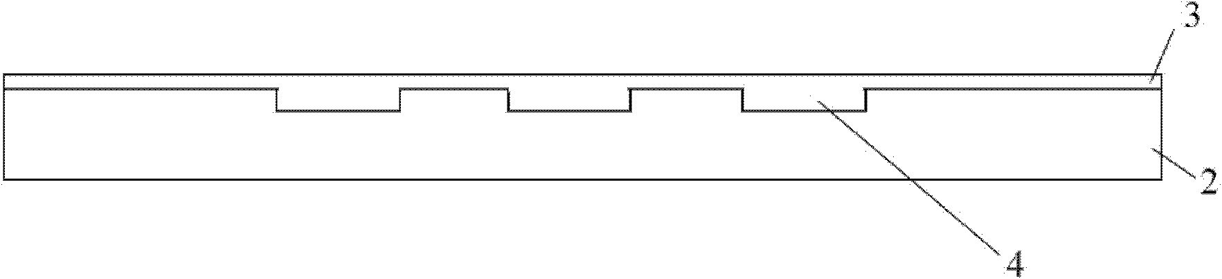
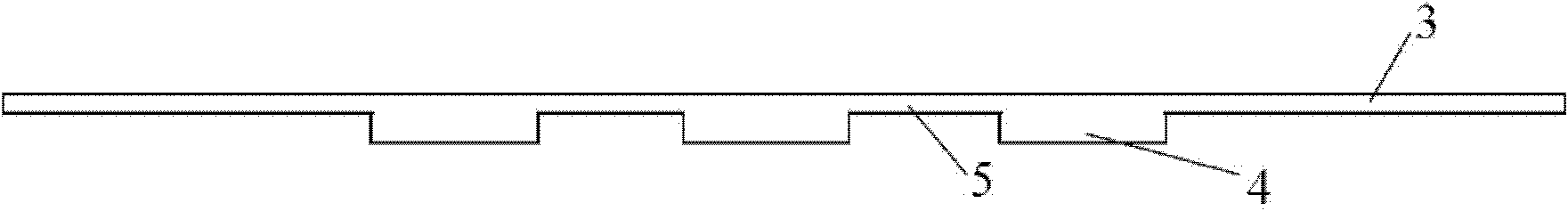
[0019] A packaging method for a wafer-level solid-state image sensor, comprising the following steps: a first step, etching a microgroove ring array on a silicon wafer (such as a 4-inch wafer), thereby obtaining a silicon wafer mold; the microcavity is circular or square, and the process for preparing the pattern structure on the silicon wafer is one of wet etching process, reactive ion etching (RIE) process or deep reactive ion etching (DRIE). In the second step, the borosilicate glass wafer is bonded to the above-mentioned silicon wafer mold under vacuum (5E~5Pa) conditions, so that the micro-groove ring of the silicon wafer mold is sealed; in the present invention, the glass is Pyrex7740 For glass, the bonding method used is anodic bonding, and the anodic bonding conditions are: voltage 600V-800V, temperature 300°C-500°C. The third step is to heat the bonded disc above the softening point of the glass and keep it warm for a certain period of time. The atmospheric pressure o...


PUM


Abstract

The invention provides a method for packaging a wafer level solid-state image sensor. The method comprises the following steps of: etching a microgroove ring array on a silicon wafer to obtain a silicon wafer mold; bonding a boron silicon glass wafer and the silicon wafer mold under vacuum conditions so as to seal the microgroove rings of the silicon wafer mold; heating the bonded wafer to a temperature above a glass softening point and keeping the temperature for a certain period of time, molding the softened glass to obtain a glass bulge loop through atmosphere of an external environment, cooling to solidify the glass and annealing; removing the silicon wafer mold to obtain a glass wafer with a glass bulge loop and a planar optical window; and after alignment, adhering the glass bulge loop and the planar optical window at an end of the glass bulge loop through an adhesive to seal the solid-state image sensor, and obtaining the packaged solid-state image sensor through a back thinning process. The method has the characteristics that: the method has a simple process flow, low cost, controllable height, high degree of parallelism and high yield.

Description

Technical field [0001] The present invention involves a Moems (micro -optical electromechanical system) packaging technology, especially the packaging method of a round -chip -class solid image sensor. Background technique [0002] Nowadays, for mobile terminal devices such as PDA, laptop, and mobile phones, people have played an increasingly important role in product design and manufacturing technology in multi -functional and low -cost needs.In recent years, a micro video camera module has been equipped with a micro -video camera module on mobile phones and other portable consumer electronics.In the mobile phone, in addition to its main features, the camera function is considered by users and mobile phone manufacturers as the core function.The industry has invested a lot of energy to improve and optimize the manufacturing process of mobile phone cameras.Wafer Level Camera is considered a technology that can meet these needs. [0003] The continuous increase in the resolution of...

Claims


Application Information

Patent Timeline
Patent Type & Authority Applications(China)
IPC IPC(8): B81C1/00H01L27/146
Inventor 尚金堂秦顺金于慧蒯文林
Owner SOUTHEAST UNIV
Why Eureka
Try Eureka