Sapphire substrate polishing device and process

A sapphire substrate and polishing device technology, applied in surface polishing machine tools, grinding/polishing equipment, manufacturing tools, etc., can solve the problems of reduced flatness, reduced chip reliability, increased leakage current, etc., and improved accuracy , the effect of improving polishing efficiency

Active Publication Date: 2012-06-27
保山鑫隆电子科技有限公司
View PDF7 Cites 12 Cited by
  • Summary
  • Abstract
  • Description
  • Claims
  • Application Information

AI Technical Summary

Problems solved by technology

CMP technology mainly uses polyurethane and non-woven soft polishing discs. Although the modified layer and surface roughness of the polished surface can meet the requirements for the use of LED substrates, the elastic deformation of the soft polishing discs during the polishing process causes the workpiece The surface pressure distribution is uneven, which often causes the wafer to "sag", and the polishing disc is gradually "glazed" due to the repeated friction of the abrasive grains during use, and the flatness is gradually reduced.
In CMP technology, a good polishing effect can be obtained by accurately controlling the particle size, concentration, hardness, pH value and temperature of the polishing liquid in the polishing liquid, but it is difficult to comprehensively control these parameters in the actual operation process and the polishing liquid It is easy to t

Method used


Image

  • Sapphire substrate polishing device and process
  • Sapphire substrate polishing device and process
  • Sapphire substrate polishing device and process

Examples


Embodiment 1

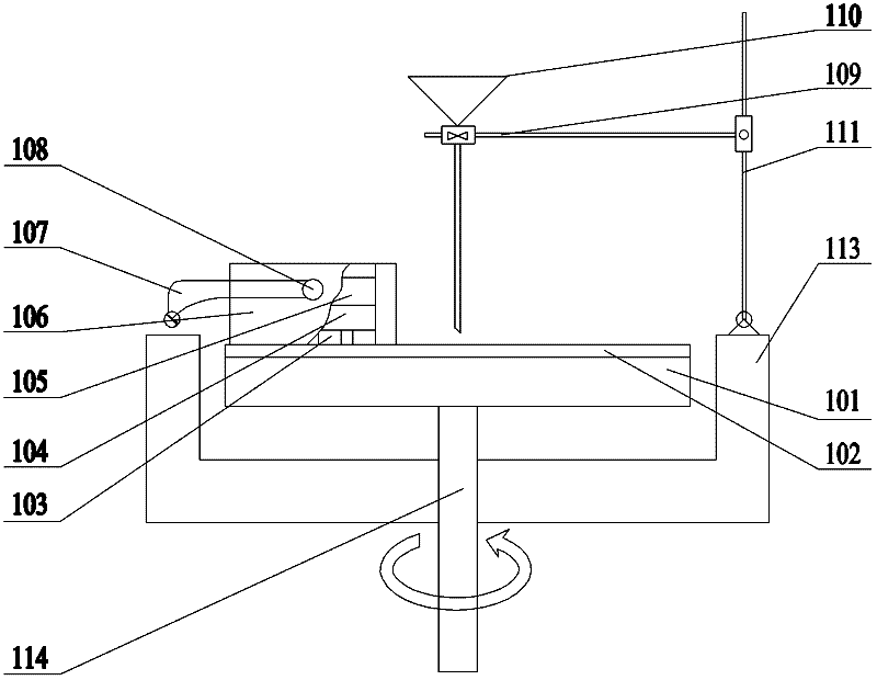
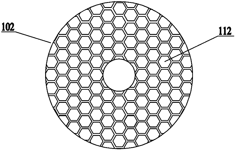
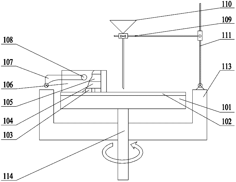
[0033] a, the 9Cr18 stainless steel polishing table 101 of Φ 380mm is installed on the rotating shaft 114 of the polishing device, and the crystal wafer 112 of 20mm * 20mm * 1mm is adhered on the polishing table 101 with ultraviolet glue, and the gap between the sheets is 0.5mm. into a crystal polishing pad 102;

[0034] b. Fix the abrasive supply mechanism on the frame 113, add 450ml of high-purity SiO with a particle size of 70nm 2 powder;

[0035] c. Start the rotating shaft 114 of the polishing table 101 to keep the rotating speed of the polishing table 101 at 30 r / min. Open the material control valve of the abrasive supply mechanism to make SiO 2Abrasives are continuously supplied to the crystal polishing pad 102 at a flow rate of 6ml / min, and after 10 minutes, the rotating shaft 114 and the abrasive supply mechanism are closed to evenly distribute the abrasives on the crystal polishing pad 102 in advance;

[0036] d, 4 pieces of sapphire substrates 103 to be polished ...

Embodiment 2

[0040] a, the 9Cr18 stainless steel polishing table 101 of Φ 380mm is installed on the polishing device rotating shaft 114, the regular hexagonal crystal chip 112 of side length 15mm, thickness 1mm is adhered on the polishing table 101 with ultraviolet glue, and the gap between sheet and sheet is 1mm, glued into a crystal polishing pad 102;

[0041] b. Fix the abrasive supply mechanism on the frame 113, add 350ml of high-purity SiO with a particle size of 80nm 2 powder;

[0042] c. Start the rotating shaft 114 of the polishing table 101 to keep the rotating speed of the polishing table 101 at 60 r / min. Open the material control valve of the abrasive supply mechanism to make SiO 2 Abrasives are continuously supplied to the crystal polishing pad 102 at a flow rate of 4ml / min. After 15 minutes, the rotating shaft 114 and the abrasive supply mechanism are closed, and the abrasives are evenly distributed on the crystal polishing pad 102 in advance;

[0043] d, 4 pieces of sapphi...

Embodiment 3

[0047] a, the 9Cr18 stainless steel polishing table 101 of Φ 380mm is installed on the polishing device rotating shaft 114, and the regular octagon crystal chip 112 of side length 10mm, thickness 1mm is adhered on the polishing table 101 with ultraviolet glue, and the gap between sheet and sheet is 2mm, glued into a crystal polishing pad 102;

[0048] b. Fix the abrasive supply mechanism on the frame 113, and add 300ml of high-purity SiO with a particle size of 90nm 2 powder;

[0049] c. Start the rotating shaft 114 of the polishing table 101 to keep the rotating speed of the polishing table 101 at 90 r / min. Open the material control valve of the abrasive supply mechanism to make SiO 2 Abrasives are continuously supplied to the crystal polishing pad 102 at a flow rate of 3ml / min. After 20 minutes, the rotating shaft 114 and the abrasive supply mechanism are closed, and the abrasives are evenly distributed on the crystal polishing pad 102 in advance;

[0050] d, 4 pieces of ...


PUM

PropertyMeasurementUnit
Thicknessaaaaaaaaaa
Flatnessaaaaaaaaaa
Surface roughnessaaaaaaaaaa

Abstract

The invention discloses a sapphire substrate polishing device and a polishing process. A rotating shaft is rotatably mounted on a frame, a polishing table is fixed to the top end of the rotating shaft, a crystal polishing pad is fixed to the upper surface of the polishing table, an abrasive feeding mechanism is arranged above the crystal polishing pad, a fixing ring is mounted on a mechanical armthrough a rubber wheel, a substrate fixing disk is arranged in the fixing ring, a pressing mechanism for pressing a sapphire substrate fixed by the substrate fixing disk towards the crystal polishingpad is arranged above the substrate fixing disk, the crystal polishing pad is formed by adhering crystal chips of the same thickness onto the upper surface of the polishing table through ultraviolet glue, and the gap between each two adjacent crystal chips ranges from 0.5mm to 2mm. After polishing, the planeness of the sapphire substrate is smaller than 5 micrometers, the surface roughness of thesapphire substrate is smaller than 0.3 nanometer, the surface of the substrate is not provided with complicated products, complicated post cleaning is omitted, cost is saved, and the rate of finishedproducts is increased.

Description

technical field [0001] The invention relates to the field of semiconductor materials. The invention discloses a sapphire substrate polishing device, and the invention also discloses a sapphire substrate polishing process. Background technique [0002] With the sharp increase in the demand for high-brightness LEDs in the field of lighting engineering, it has driven the development of the domestic sapphire substrate material preparation industry. Since the sapphire crystal (α—Al 2 o 3 ) has remarkable characteristics such as high temperature resistance, corrosion resistance, and wide light transmission band, and is the preferred substrate material for externally extended GaN. , especially the nanoscale polishing of the wafer surface brings many technical difficulties. In order to cope with the ultra-smooth and non-damaging requirements on the surface of product substrate materials put forward by the development of optoelectronic technology, the sapphire substrate must be fi...

Claims


Application Information

Patent Timeline
IPC IPC(8): B24B29/02
Inventor 柳祝平黄小卫王联
Owner 保山鑫隆电子科技有限公司
Why Eureka
Try Eureka