ZnO substrate epitaxy structure, manufacture method thereof and ZnO substrate chip structure

A technology of epitaxial structure and manufacturing method, which is applied in the direction of electrical components, circuits, semiconductor devices, etc., and can solve problems such as blue light spot, low light extraction efficiency, yellow phosphor coating thickness, yellow aperture, etc.

Active Publication Date: 2014-06-11
内蒙古华延芯光科技有限公司
View PDF1 Cites 0 Cited by
  • Summary
  • Abstract
  • Description
  • Claims
  • Application Information

AI Technical Summary

Problems solved by technology

At present, blue light LEDs are usually used to excite non-transparent yellow phosphor powder to produce white light LEDs through wavelength conversion. Since the continuous lighting of blue light LEDs will cause temperature rise and wavelength conversion materials will degrade, when the light emitted by blue light chips passes through yellow phosphor powder Phenomena such as scattering and absorption will occur, so that the light extraction efficiency is not high. At the same time, due to the uneven coating thickness of the yellow phosphor powder, it will also cause problems such as yellow apertures, blue spots, and inconsistent color temperature of white light. The white light LED produced by powder has poor color rendering and poor stability

Method used


Image

  • ZnO substrate epitaxy structure, manufacture method thereof and ZnO substrate chip structure
  • ZnO substrate epitaxy structure, manufacture method thereof and ZnO substrate chip structure

Examples


Embodiment Construction

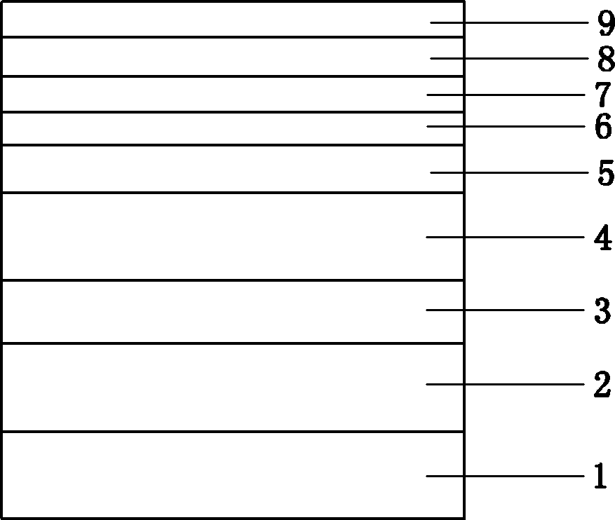
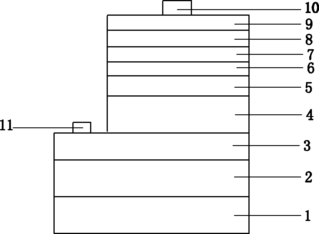
[0028] Such as figure 1 As shown, a ZnO substrate epitaxial structure includes an epitaxial wafer, and the epitaxial wafer includes a ZnO substrate 1, a GaN transition layer 2, a first N-GaN contact layer 3, doped Si and Zn In 0.2 Ga 0.8 N / GaN multi-quantum well light-emitting layer 4, first P-GaN contact layer 5, N-GaN cascade layer 6, second N-GaN contact layer 7, In doped with Si and Zn 0.49 Ga 0.51 N / GaN multi-quantum well light-emitting layer 8 and the second P-GaN contact layer 9 . ZnO substrate is a nanoscale material with wide energy band gap, high refractive index, high light transmittance, and has excellent fluorescence effect and electroluminescent function.

[0029] Wherein, the thickness of the ZnO substrate 1 is 50-200um, preferably 100um.

[0030] Wherein, the thickness of the GaN transition layer 2 is 10-100 nm, preferably 50 nm.

[0031] Wherein, the thicknesses of the first N-GaN contact layer 3 and the second N-GaN contact layer 7 are both 200-1000 nm,...


PUM

PropertyMeasurementUnit
thicknessaaaaaaaaaa
thicknessaaaaaaaaaa
thicknessaaaaaaaaaa

Abstract

The invention discloses a ZnO substrate epitaxy structure, a manufacture method of the ZnO substrate epitaxy structure and a ZnO substrate chip structure containing the epitaxy structure. An epitaxial wafer of the epitaxy structure comprises a ZnO substrate, a GaN transition layer, a first N-GaN contact layer, an Si and Zn doped In0.2Ga0.8N / GaN multiple quantum well luminescent layer, a first P-GaN contact layer, an N-GaN cascading layer, a second N-GaN contact layer, an Si and Zn doped In0.49Ga0.51N / GaN multiple quantum well luminescent layer and a second P-GaN contact layer, which are sequentially arranged from bottom to top. The ZnO substrate epitaxy structure and the chip structure disclosed by the invention do not need to be coated with fluorescent powder, so that the constraint of the fluorescent powder is fundamentally removed, and the ZnO substrate epitaxy structure has good luminescent quality and good color rendering property, the working stability is improved, the service life is prolonged, and the packaging process is reduced. In the ZnO substrate epitaxy structure and the ZnO substrate chip structure disclosed by the invention, the production technology of the whole industrial chain from the white light LED epitaxy, chips, packaging and application can be simplified; and the production efficiency is high and the ZnO substrate epitaxy structure and the chip structure are suitable for large-batch production.

Description

technical field [0001] The invention relates to the technical field of semiconductor lighting, in particular to a ZnO substrate epitaxial structure and a manufacturing method thereof, and a ZnO substrate chip structure including the epitaxial structure. Background technique [0002] White light LED has many advantages such as energy saving, environmental protection, long life, and can work at high speed. Its application is becoming wider and wider, and the government is vigorously promoting it. At present, blue light LEDs are usually used to excite non-transparent yellow phosphor powder to produce white light LEDs through wavelength conversion. Since the continuous lighting of blue light LEDs will cause temperature rise and wavelength conversion materials will degrade, when the light emitted by blue light chips passes through yellow phosphor powder Phenomena such as scattering and absorption will occur, so that the light extraction efficiency is not high. At the same time, d...

Claims


Application Information

Patent Timeline
Patent Type & Authority Patents(China)
IPC IPC(8): H01L33/06H01L33/28
Inventor 汪英杰吉爱华王凯敏
Owner 内蒙古华延芯光科技有限公司
Why Eureka
Try Eureka