
Method for preparing FeSe superconducting thin film by post-selenization treatment

A technology of superconducting thin film and processing method, which is applied in the direction of ion implantation plating, metal material coating process, coating, etc., can solve the problems of no major breakthrough, high maintenance cost, and reduced yield, and achieve the goal of being independent of size. Limit, reduce impurity phase, reduce stress effect

Active Publication Date: 2013-06-19
GRIMAT ENG INST CO LTD
View PDF5 Cites 2 Cited by
  • Summary
  • Abstract
  • Description
  • Claims
  • Application Information

AI Technical Summary

Problems solved by technology

[0002] In early 2008 superconductor LaFeAsO 1-x f x The discovery of the new iron-based superconductor triggered a new wave of research. The main reason is not only that there has been no major breakthrough in the performance of the previous copper-based superconductor for 20 years, but more importantly, the iron-based superconductor may make the controversy Long-standing theory of superconductivity has new explanation
Among them, the equipment of MBE is too expensive and the maintenance cost is high; laser pulse sputtering is only suitable for preparing small-sized samples
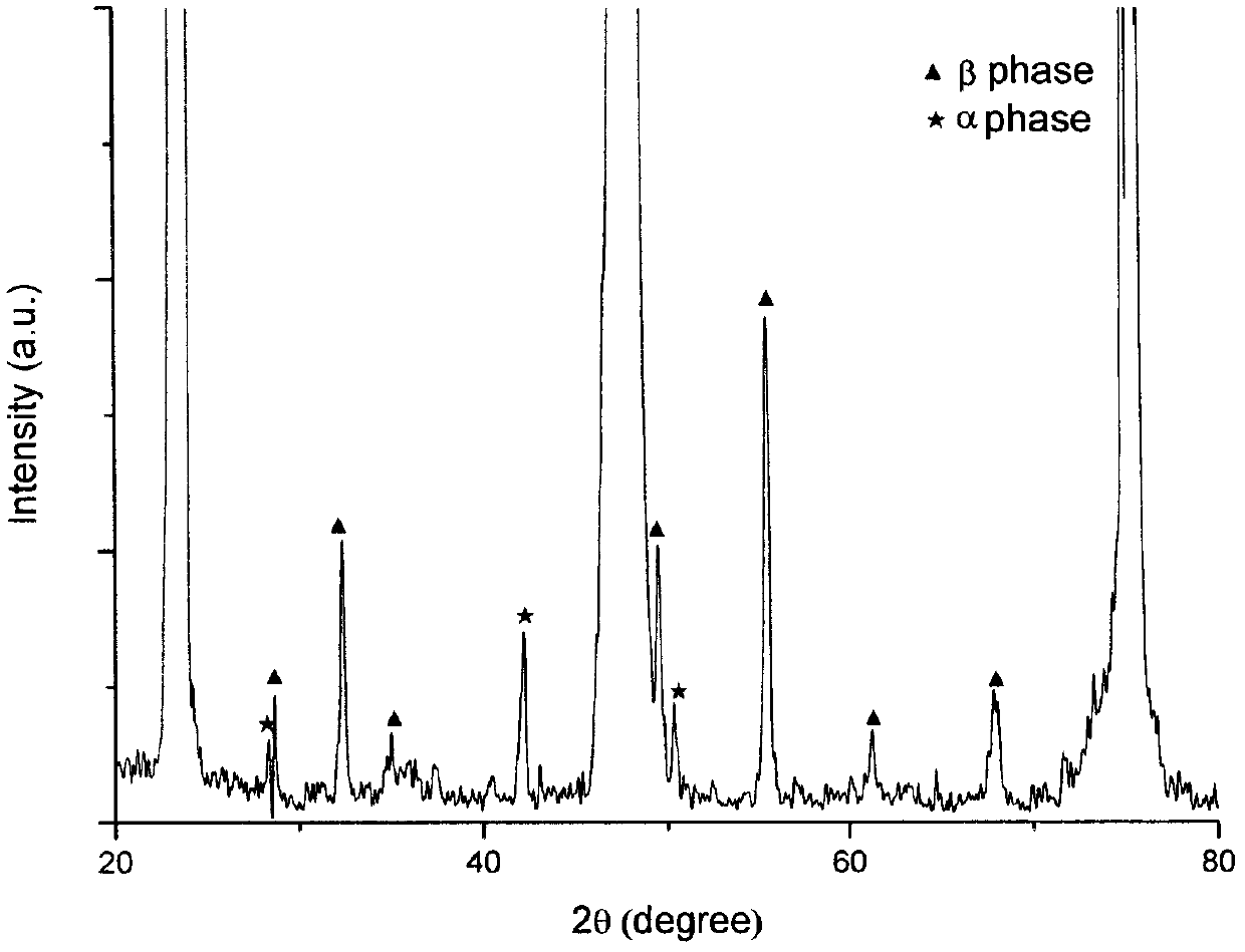
In the post-selenization method used in the past, the selenium vapor reaction diffusion is extruded into the Fe film, and some α phases without superconducting properties will be formed to weaken the influence of lattice distortion, accompanied by pores and cracks, which will reduce the yield

Method used


Image

  • Method for preparing FeSe superconducting thin film by post-selenization treatment
  • Method for preparing FeSe superconducting thin film by post-selenization treatment
  • Method for preparing FeSe superconducting thin film by post-selenization treatment

Examples


Embodiment 1

[0026] In the first step, lanthanum aluminate (LaAlO 3 ) the surface of the single crystal substrate is cleaned with acetone and alcohol;

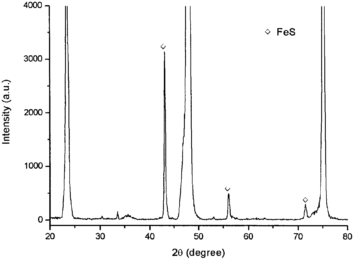
[0027] The second step is to deposit a layer of FeS film with a thickness of about 4 μm on the cleaned LAO single crystal substrate by reactive sputtering film deposition technology. Specific sputtering deposition conditions: substrate temperature 400°C, target material is Fe target with a purity of 99.99% , back vacuum degree 5.0×10 -3 Pa, H 2 The S reaction gas flow rate is 40 sccm, the sputtering power is 100 W, and the target base distance is 40 mm.

[0028] The third step is to use a semi-automatic electro-optic balance to weigh 3.8 mg of amorphous elemental selenium. The elemental selenium is weighed by a semi-automatic electro-optic balance, and the deposited FeS film is placed in a quartz tube with a diameter of 20 mm. The combination of pump and mechanical pump is used for pumping, the other end is heated by a high-temperature ...

Embodiment 2

[0031] In the first step, lanthanum aluminate (LaAlO 3 ) the surface of the single crystal substrate is cleaned with acetone and alcohol;

[0032] The second step is to deposit a layer of FeS film with a thickness of about 10 μm on the cleaned LAO single crystal substrate by reactive sputtering film deposition technology. Specific sputtering deposition conditions: substrate temperature 500°C, target material is Fe target with a purity of 99.99% , back vacuum degree 4.0×10 -3 Pa, H 2 The S reaction gas flow rate is 20 sccm, the sputtering power is 120 W, and the target base distance is 60 mm.

[0033] The third step is to use a semi-automatic electro-optic balance to weigh 16 mg of amorphous elemental selenium. The elemental selenium is weighed by a semi-automatic electro-optic balance, and placed in a quartz tube with a diameter of 20 mm together with the deposited FeS film, and vacuum-sealed, that is, a diffusion pump is used at one end The combination of mechanical pump i...

Embodiment 3

[0036] In the first step, lanthanum aluminate (LaAlO 3 ) the surface of the single crystal substrate is cleaned with acetone and alcohol;

[0037] The second step is to deposit a layer of FeS film with a thickness of about 3 μm on the cleaned LAO single crystal substrate using reactive sputtering film deposition technology. Specific sputtering deposition conditions: substrate temperature 200 ° C, target material is Fe target with a purity of 99.99% , back vacuum degree 6.0×10 -3 Pa, H 2 The S reaction gas flow rate is 30 sccm, the sputtering power is 60 W, and the target base distance is 50 mm.

[0038] In the third step, 0.2 mg of amorphous elemental selenium was weighed with a semi-automatic electro-optic balance, and placed in a quartz tube with a diameter of 20 mm together with the deposited FeS film, and vacuum-sealed, and the vacuum degree in the quartz tube was 1×10 -3 Pa.

[0039] In the fourth step, the sealed quartz tube is placed in a heating furnace to raise th...


PUM

PropertyMeasurementUnit
thicknessaaaaaaaaaa
diameteraaaaaaaaaa

Abstract

The invention relates to a method for preparing a FeSe superconducting thin film by post-selenization treatment;in the method, a FeSe thin film is deposited by reactive sputtering; the method comprises the following steps: performing surface treatment of a substrate; sputtering and depositing a FeSe thin film on the substrate by reactive sputtering film deposition technology; putting both the FeSe thin film and amorphous simple substance selenium in a quartz tube, performing vacuum sealing; putting the sealed quartz tube in a heating furnace, heating to perform a selenization reaction to obtain the FeSe thin film. With the invention, the stress generated after selenization treatment is significantly reduced; impurity phases, air pores and cracks generated as a result of excessive distortion energy are reduced; and excellent superconductive performance of the thin film is brought into play. Additionally, when compared with commonly-used pulse laser deposition methods, the preparation method combining reactive sputtering with improved selenization treatment has great advantages in cost control, and is not restricted by dimensions.

Description

technical field [0001] The invention relates to a method for preparing an Fe-based superconducting thin film, in particular to a novel post-selenization method for preparing a FeSe superconducting thin film. The FeSe thin film is prepared by selenizing the FeS thin film. Background technique [0002] In early 2008 superconductor LaFeAsO 1-x f x The discovery of the new iron-based superconductor triggered a new wave of research. The main reason is not only that there has been no major breakthrough in the performance of the previous copper-based superconductor for 20 years, but more importantly, the iron-based superconductor may make the controversy The long-standing theoretical mechanism of superconductivity has a new explanation. In the same year, β-FeSe, which has the simplest structure among iron-based superconductors and does not contain As highly toxic substances, was synthesized. Its superconducting transition temperature Tc can reach 8K, and it can be raised to 27K a...

Claims


Application Information

Patent Timeline
Patent Type & Authority Patents(China)
IPC IPC(8): C23C14/00C23C14/06C23C14/58
Inventor 柴青林华志强王磊屈飞李弢
Owner GRIMAT ENG INST CO LTD
Learn More